Semiconductor light-emitting device and its manufacturing method

a technology of semiconductor light-emitting devices and manufacturing methods, which is applied in the direction of lasers, semiconductor laser structural details, semiconductor lasers, etc., can solve the problems of limiting the minimal size of the above-mentioned semiconductor light-emitting devices and inevitably increasing the size of the light-emitting device array, and achieves small size and sufficient mechanical strength.

Inactive Publication Date: 2010-05-18
HAMAMATSU PHOTONICS KK
View PDF35 Cites 118 Cited by
  • Summary
  • Abstract
  • Description
  • Claims
  • Application Information

AI Technical Summary

Benefits of technology

[0005]It is an object of the present invention to provide a semiconductor light-emitting device which has a sufficient mechanical strength and can be made small, and to provide a method of manufacturing the same.

Problems solved by technology

Since the part maintaining the substrate thickness exists, however, there is a limit to the minimal size of the above-mentioned semiconductor light-emitting devices.
In particular, when forming a light-emitting device array by arranging a plurality of light-emitting parts a row, the pitch between the light-emitting parts is hard to narrow, which inevitably increases the size of the light-emitting device array.

Method used


Image

  • Semiconductor light-emitting device and its manufacturing method
  • Semiconductor light-emitting device and its manufacturing method
  • Semiconductor light-emitting device and its manufacturing method

Examples


first embodiment

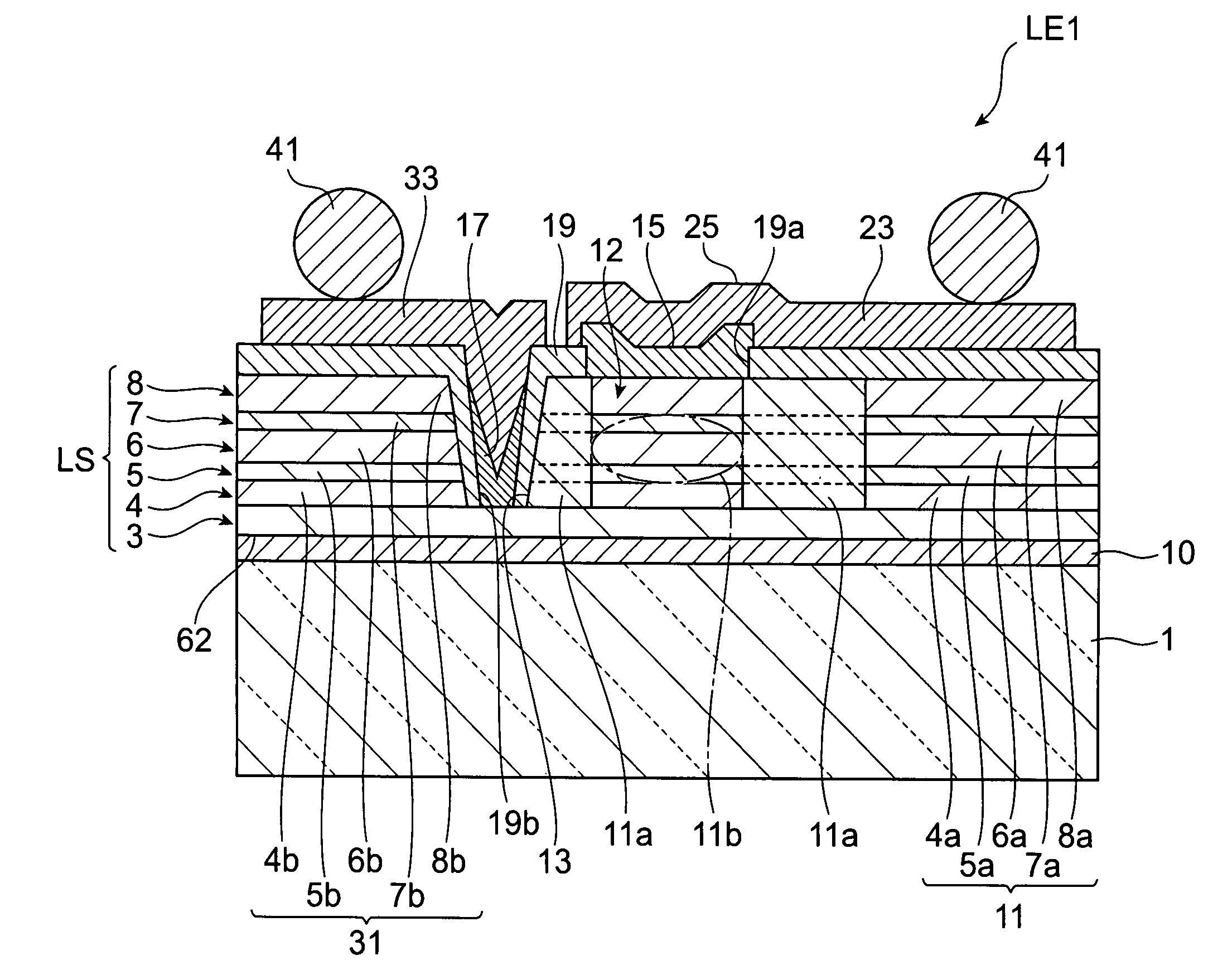
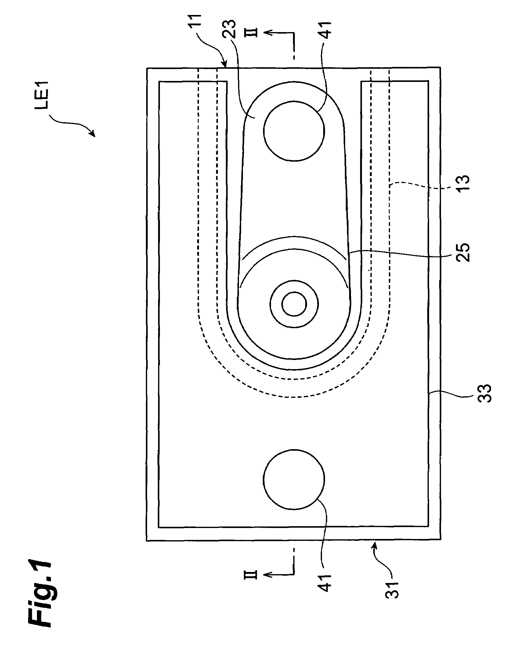
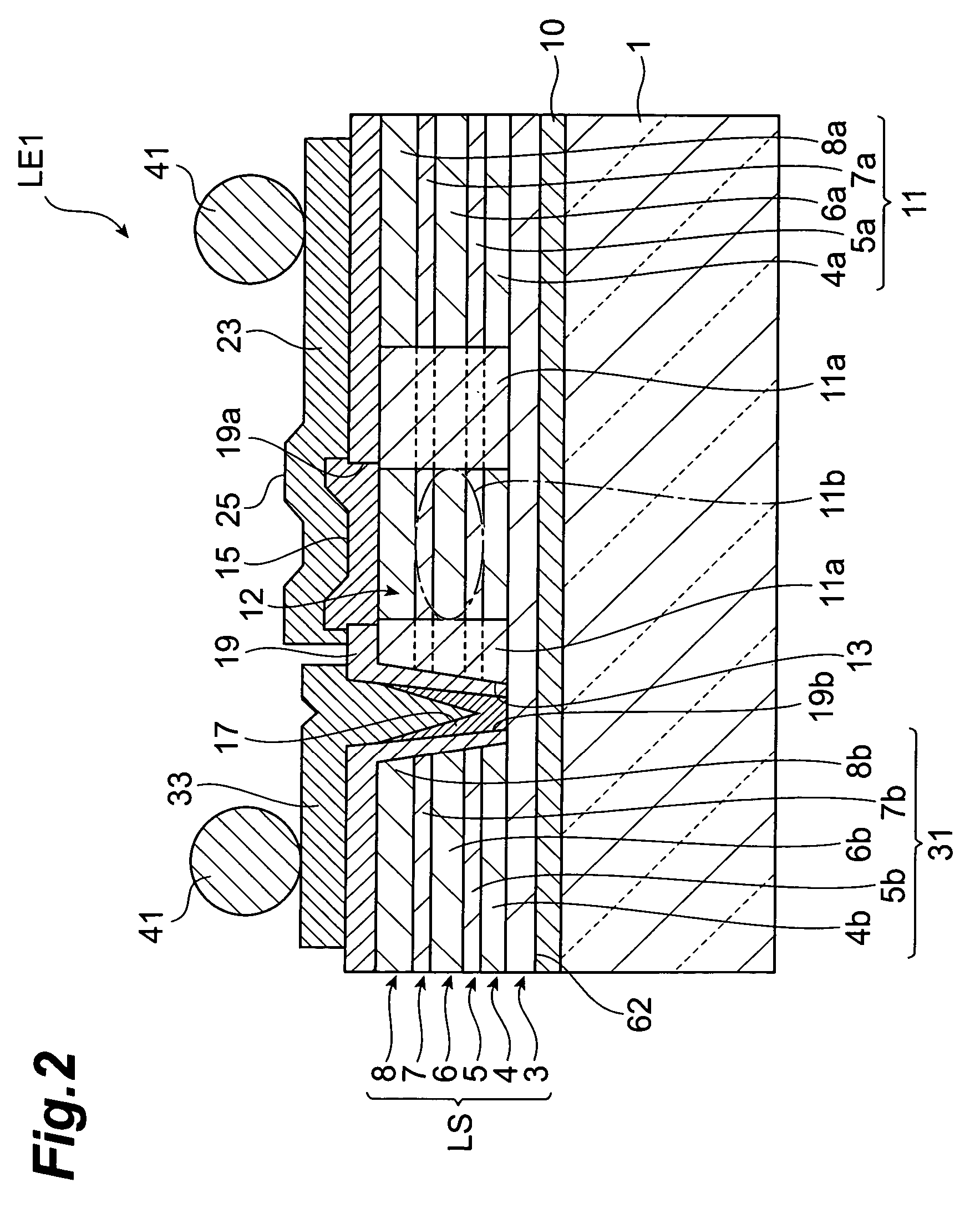
[0044]FIG. 1 is a schematic plan view showing a semiconductor light-emitting device in accordance with the first embodiment. FIG. 2 is a schematic sectional view taken along line II-II in FIG. 1.

[0045]The semiconductor light-emitting device LE1 has a multilayer structure LS and a glass substrate 1. This semiconductor light-emitting device LE1 is a vertical cavity surface emitting laser (VCSEL) of back emission type which emits light from the side of the glass substrate 1. The semiconductor light-emitting device LE1 is a light-emitting device for short-distance optical communications in the wavelength band of 0.85 μm, for example.

[0046]The multilayer structure LS includes a p-type (first conductive type) contact layer 3, a p-type first distributed Bragg reflector (DBR) layer 4, a p-type first cladding layer 5, an active layer 6, an n-type (second conductive type) second cladding layer 7, and an n-type second DBR layer 8. The multilayer structure LS generates light when a voltage is a...

second embodiment

[0105]FIG. 11 is a schematic sectional view showing the structure of a semiconductor light-emitting device in accordance with the second embodiment. The semiconductor light-emitting device LE2 differs from the semiconductor light-emitting device LE1 of the first embodiment in that the glass substrate 1 is formed with a lens part 72a.

[0106]The semiconductor light-emitting device LE2 comprises a multilayer structure LS and a glass substrate 1. The semiconductor LE1 is a VCSEL of back emission type which emits light from the side of the glass substrate 1. The semiconductor light-emitting device LE1 is a light-emitting device for short-distance optical communications in the wavelength band of 0.85 μm, for example.

[0107]The rear face 72 of the glass substrate 1 is formed with the lens part 72a for receiving the light emitted from the multilayer structure LS. The other part 72b in the rear face 72 is raised from the lens part 72a. Namely, the lens part 72a is depressed from the most rais...


PUM


Abstract

A semiconductor light-emitting device comprises a multilayer structure and a glass substrate. The multilayer structure includes a plurality of laminated compound semiconductor layers and generates light. The multilayer structure has a light exit face for emitting the generated light, whereas the glass substrate optically transparent to the light is bonded to the light exit face by a film made of silicon oxide.

Description

TECHNICAL FIELD[0001]The present invention relates to a semiconductor light-emitting device and a method of manufacturing the same.BACKGROUND ART[0002]Recently, as CPUs have been driven at a higher frequency (e.g., 10 GHz or higher), attention has been focused on optical interconnection techniques which transmit signals within and between system apparatus by light. Optical semiconductor devices such as semiconductor photodetecting devices and semiconductor light-emitting devices are used in the optical interconnection techniques.[0003]Japanese Patent Application Laid-Open Nos. HEI 2-128481, HEI 10-200200, and HEI 11-46038 disclose semiconductor light-emitting devices of so-called back emission type each comprising a substrate and a plurality of compound semiconductor layers laminated on one principal surface of the substrate, while light is emitted from the other principal surface of the substrate. For the following purposes, the part of substrate positioned under the light-emitting...

Claims


Application Information

Patent Timeline
Patent Type & Authority Patents(United States)
IPC IPC(8): H01L33/00H01S5/02H01S5/026H01S5/042H01S5/183H01S5/20H01S5/30H01S5/42
CPCH01S5/423H01S5/0422H01S5/18305H01L33/20H01S5/0208H01S5/0215H01S5/0217H01S5/0224H01S5/02248H01S5/02272H01S5/0425H01S5/18308H01S5/18388H01S5/2063H01S5/305H01S5/3054H01S5/0207H01L2224/11H01S5/04257H01S5/0234H01S5/02325H01S5/0237
Inventor TANAKA, AKIMASA
Owner HAMAMATSU PHOTONICS KK
Why Eureka
Try Eureka