Organic light emitting display with auxiliary electrode line and method of fabricating the same

a technology of light-emitting display and electrode line, which is applied in the field of organic light-emitting display (oled), can solve the problems of metal line damage by etchant or developing agent, pixel shrinkage phenomenon, and inability to smoothly reflowed organic layer, so as to minimize the organic layer in the pixel region, improve product reliability, and prevent pixel shrinkage

Active Publication Date: 2010-06-01
SAMSUNG DISPLAY CO LTD
View PDF22 Cites 50 Cited by
  • Summary
  • Abstract
  • Description
  • Claims
  • Application Information

AI Technical Summary

Benefits of technology

[0017]The present invention, therefore, provides an OLED and a method of fabricating the same capable of improving product reliability by forming an auxiliary electrode line to be in contact with a second electrode power supply line to remove an organic layer on the auxiliary electrode line and minimize the organic layer on a pixel region, thereby preventing pixel shrinkage resulting from degradation of an organic emission layer caused by out-gassing from the organic layer.

Problems solved by technology

As a result, when curing the organic layer, the organic layer cannot be smoothly reflowed to each region and consequently the thickness of the organic layer differs in each region after curing.
Here, residual gas remaining around the first conductive pattern and an adjacent pixel region may cause a pixel shrinkage phenomenon due to degradation of the organic emission layer by out-gassing.
In addition, when the second electrode is formed to be in contact with the first conductive pattern, a metal material of the first conductive pattern of the metal line region is exposed when forming the first electrode of the pixel region, resulting in the metal line being damaged by an etchant or developing agent.

Method used


Image

  • Organic light emitting display with auxiliary electrode line and method of fabricating the same
  • Organic light emitting display with auxiliary electrode line and method of fabricating the same
  • Organic light emitting display with auxiliary electrode line and method of fabricating the same

Examples


Embodiment Construction

[0026]The present invention will now be described more fully hereinafter with reference to the accompanying drawings, in which preferred embodiments of the invention are shown.

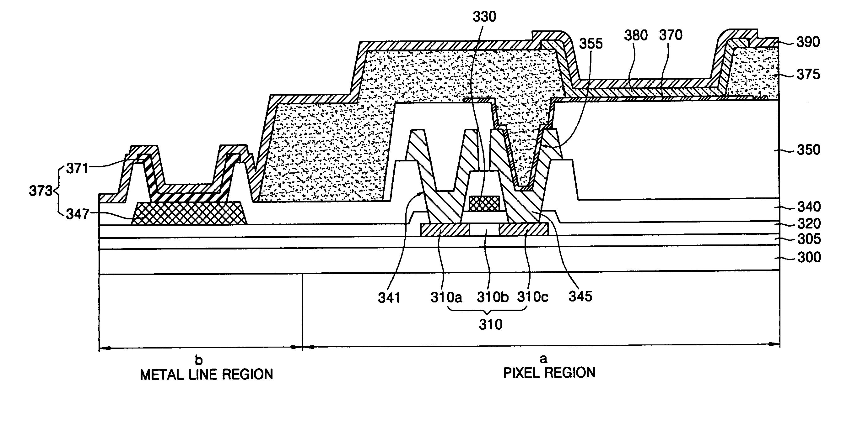
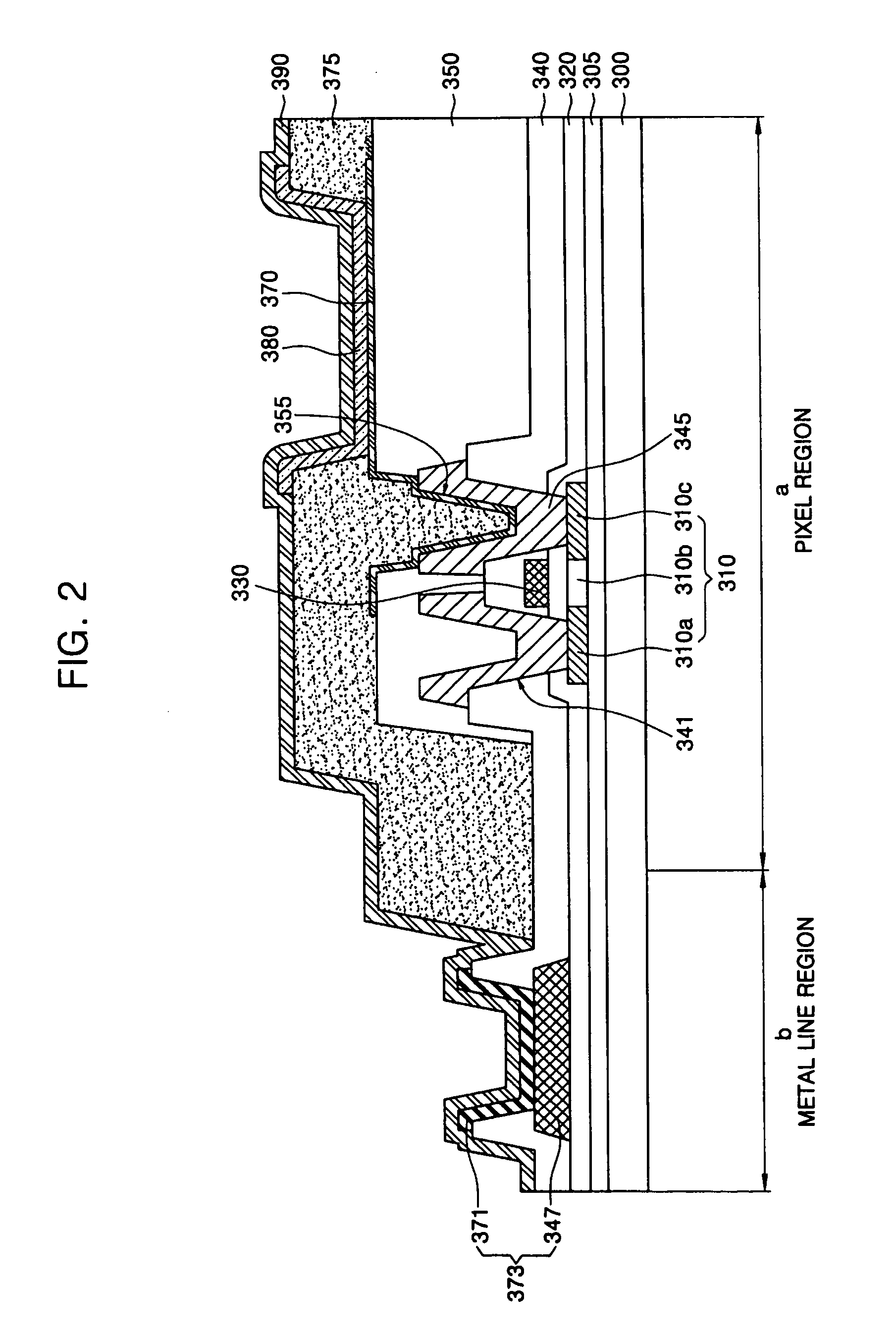
[0027]FIG. 2 is a cross-sectional view of an active OLED in accordance with the present invention.

[0028]Referring to FIG. 2, the active OLED in accordance with the present invention includes a substrate 300 having a pixel region (a) and a metal line region (b), and a buffer layer 305 is formed on the entire surface of the substrate 300. The buffer layer 305 is formed of a silicon nitride layer, a silicon oxide layer, or a double layer thereof. Polysilicon or amorphous silicon is formed in the pixel region (a) on the buffer layer 305 and then patterned to form a semiconductor layer 310 having source and drain regions 310a and 310c and a channel region 310b. Preferably, the semiconductor layer 310 is formed of polysilicon.

[0029]A gate insulating layer 320 is formed on the entire surface of the substrate includin...


PUM


Abstract

Provided are an organic light emitting display (OLED) and a method of fabricating the same capable of improving product reliability by forming an auxiliary electrode line to be in contact with a second electrode power supply line to remove an organic layer on the auxiliary electrode line and minimize the organic layer on a pixel region, thereby preventing pixel shrinkage resulting from degradation of an organic emission layer caused by out-gassing from the organic layer.

Description

CROSS-REFERENCE TO RELATED APPLICATION[0001]This application claims priority to and the benefit of Korean Patent Application No. 10-2004-0105900, filed Dec. 14, 2004, which is incorporated herein by reference in its entirety.BACKGROUND OF THE INVENTION[0002]1. Field of the Invention[0003]The present invention relates to an organic light emitting display (OLED) and a method of fabricating the same, and more particularly, to an OLED and a method of fabricating the same that is capable of improving product reliability by forming an auxiliary electrode line to be in contact with a second electrode power supply line to remove an organic layer on the auxiliary electrode line and minimize the organic layer on a pixel region, thereby preventing pixel shrinkage resulting from degradation of an organic emission layer caused by out-gassing from the organic layer.[0004]2. Description of the Related Art[0005]An organic light emitting display (OLED) is an emissive flat panel display that has bene...

Claims


Application Information

Patent Timeline
Patent Type & Authority Patents(United States)
IPC IPC(8): H01J1/62H01J63/04
CPCH01L51/5221H01L51/5206H01L27/3276H01L27/3246H10K59/123H10K59/122H10K59/131H10K59/8051H10K59/8052H10K59/80516H10K59/80522H05B33/26H05B33/10H10K50/81H10K50/82
Inventor OH, SANG-HUN
Owner SAMSUNG DISPLAY CO LTD
Why Eureka
Try Eureka