Image forming apparatus with reduced loss of electron source caused by the inert gas

a technology of electron source and forming apparatus, which is applied in the direction of vacuum obtaining/maintenance, tubes with screens, instruments, etc., can solve the problems of destroying the apparatus, affecting the flow of gas, and unable to display a bright image, so as to reduce the loss of electron sour

Inactive Publication Date: 2010-06-08
CANON KK
View PDF48 Cites 7 Cited by
  • Summary
  • Abstract
  • Description
  • Claims
  • Application Information

AI Technical Summary

Benefits of technology

[0015]It is an object of the present invention to provide an image display apparatus which can reduce the losses of electron sources caused by an inert gas existing in the panel and can exhaust the inert gas.
[0016]Moreover, it is another object of the invention to provide an image forming apparatus having a small aged deterioration and a small spatial distribution of luminance.

Problems solved by technology

The reason is that, in the case where a gas is generated in the vacuum chamber to raise the pressure therein, the rise of the pressure exerts a harmful influence on the electron source to reduce the electron emission quantity thereof, which makes it impossible to display a bright image, though the degree of the influence changes with the kind of the gas.
Furthermore, in that case, there is the possibility that an electric discharge occurs in the inside to destroy the apparatus.
Moreover, because supporting members for holding the vacuum chamber and the like are provided, the flow of gas is hindered, and the tabular image forming apparatus is in a state of being bad in conductance.
Moreover, because, for example, Ar is heavy in weight among the inert gasses, there is a problem such that, in the case where Ar is accelerated by a strong electric field after ionization, the electron sources are damaged seriously.
H05-121012, there is some possibility that the external ion pump cannot deal with a rise of a local pressure of the inert gas in the tabular image display apparatus having deteriorated conductance.
Thus, the conventional technique also has a problem of a high cost.
Moreover, in the conventional technique disclosed in U.S. Pat. No. 6,107,745, because the electron source is provided out of the image display region, the tabular image display apparatus is influenced by the conductance, and there is some possibility that the tabular image display apparatus cannot deal with a local pressure rise.
Moreover, because the arrangement of the ion pump is only out of the image region, and because the electron source for the ionization of the inert gas itself has a configuration having the possibility of being deteriorated, there is some possibility that a sufficient exhaust velocity and a sufficient total exhaust quantity cannot be obtained.
Moreover, it is difficult to apply the general CRT technique to a tabular image display apparatus.

Method used


Image

  • Image forming apparatus with reduced loss of electron source caused by the inert gas
  • Image forming apparatus with reduced loss of electron source caused by the inert gas
  • Image forming apparatus with reduced loss of electron source caused by the inert gas

Examples


example 1

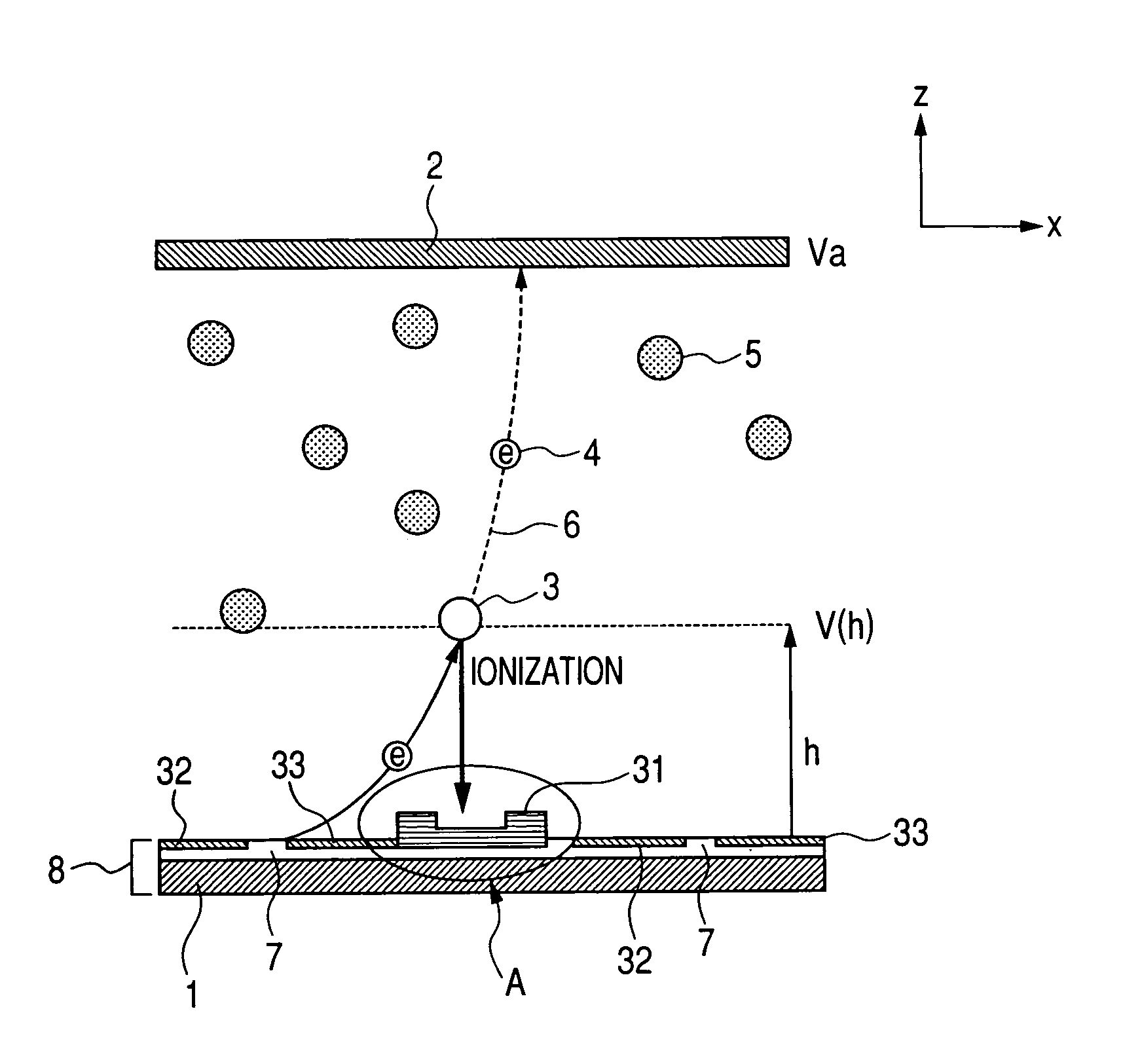
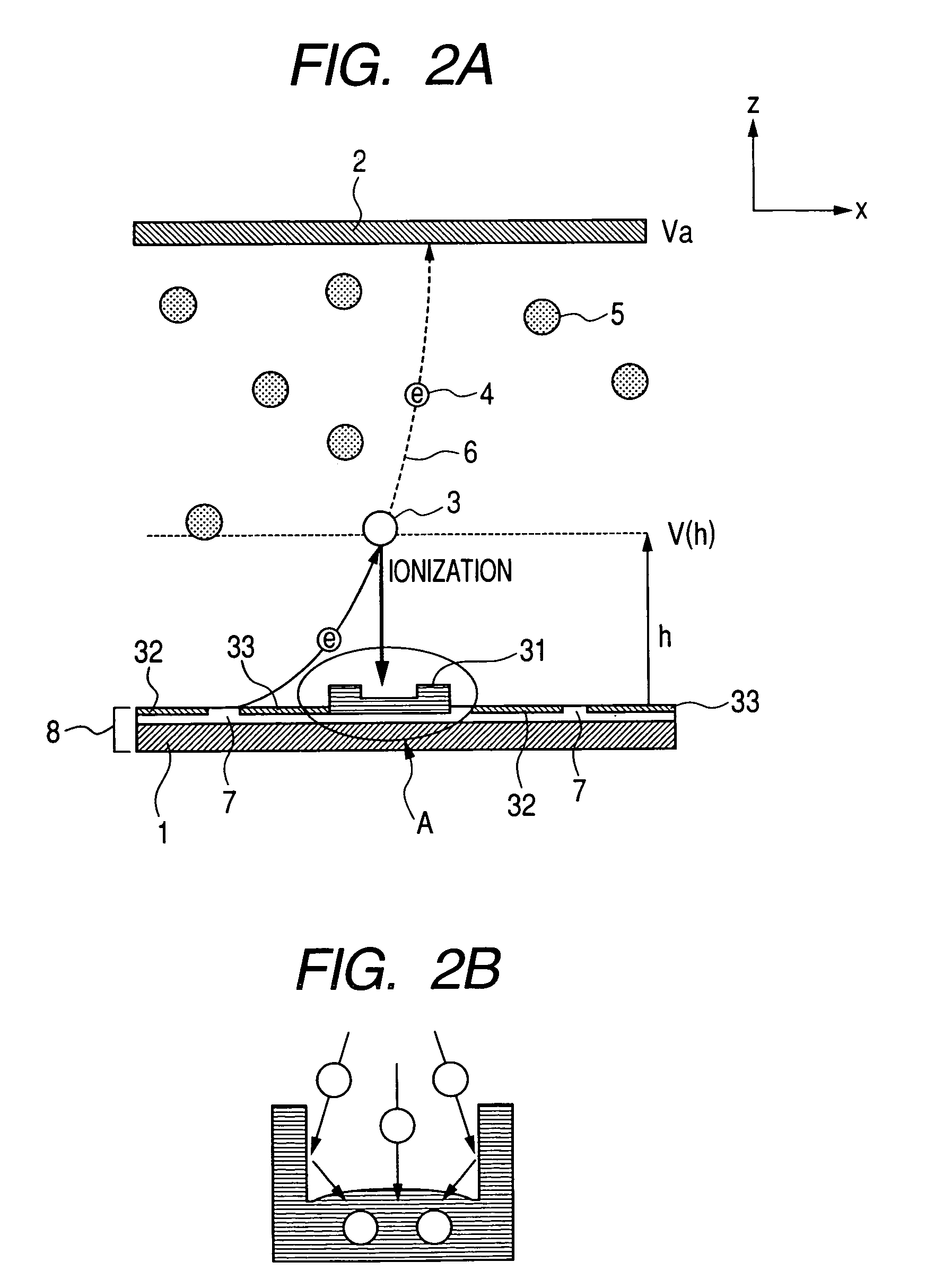
[0081]The present example was manufactured based on the embodiment shown in FIG. 1, and an enlarged view of the cross section along the line x0-x1 is shown in FIGS. 2A and 2B.

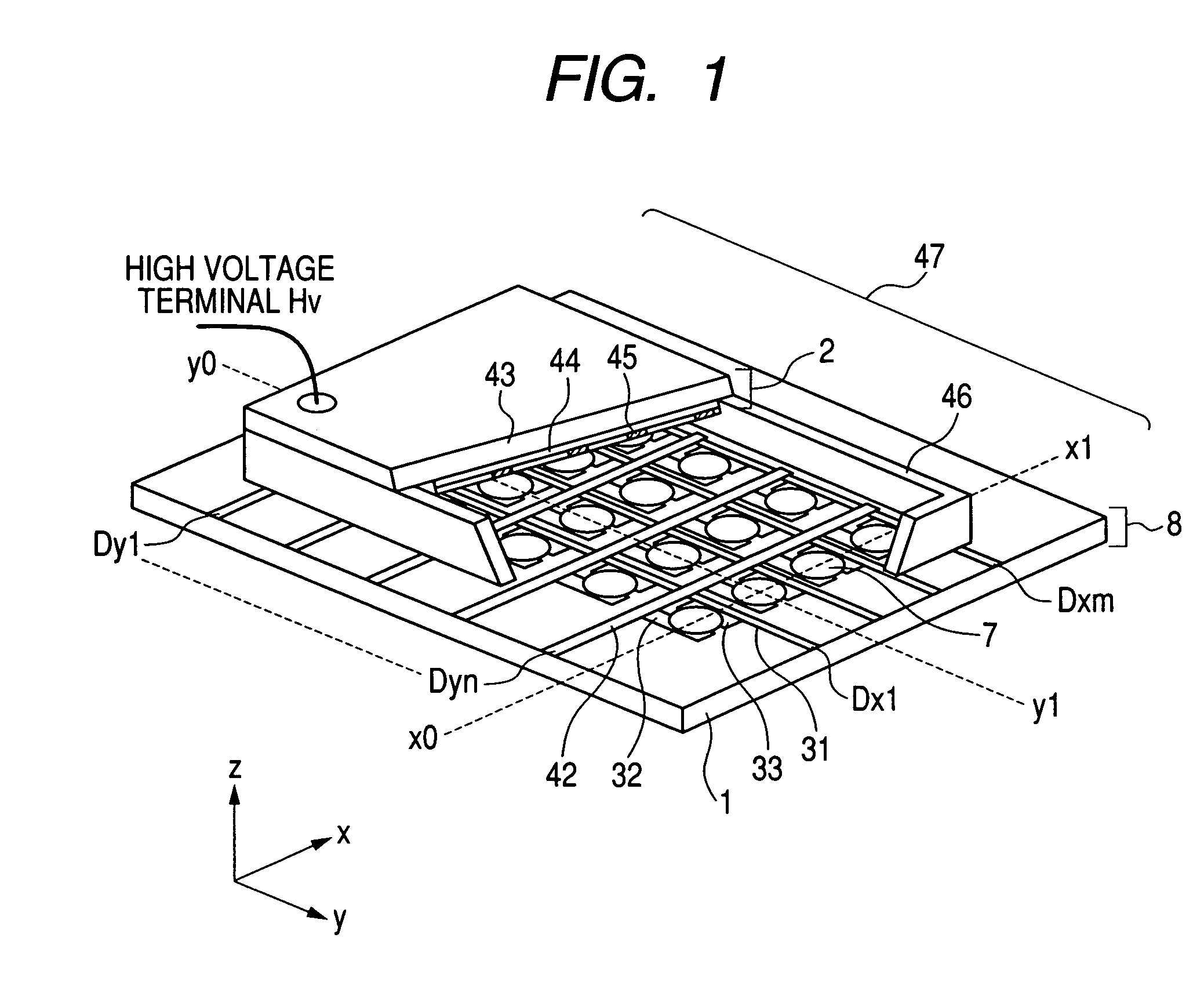
[0082]The electron beam deflection mechanism and the ion trapping mechanism of the present example are described. The column wiring 31 manufactured based on the present example was set to have a height of 25 μm and the depth of a recess of 15 μm. The width and the height of the column wiring 31 are suitably defined according to the initial velocity vectors of the electron beams, the voltage applied to the face plate 2, the distance between the face plate 2 and the rear plate 8, and the like without being limited to those of the present example. Moreover, the desirable range of recess is that of from several μm to several tens μm. After the manufacture, the voltages 0 V, 15.5 V and 10 kV were applied to the device electrodes (on the lower voltage side) 32 through the row wiring 42, the device electrodes (on the ...

example 2

[0086]FIGS. 7A and 7B are views showing a cross section of a second example of the image forming apparatus shown in FIG. 1; FIG. 7A is a view showing a part thereof; and FIG. 7B is an enlarged view of a part C shown in FIG. 7A.

[0087]The present example forms one pixel of two electron-emitting devices 7 which put the column wiring 31 between them, as shown in FIGS. 7A and 7B. For this reason, both of the two device electrodes (on the higher voltage side) 33 putting the column wiring 31 between them are electrically connected to the column wiring 31, and a higher voltage is applied to the two device electrodes 33 than a voltage applied to the device electrodes (on the lower voltage side) 32 electrically connected to the row wiring 31 shown in FIG. 1. Only the above point differs from the first example. As a result, as shown in FIGS. 7A and 7B, two electron orbits 6 cross and pass above the column wiring 31. One pixel is formed by these two electron orbits 6.

[0088]The electron beam def...

example 3

[0093]FIGS. 8A and 8B are views showing a cross section of a third example of the image forming apparatus shown in FIG. 1; FIG. 8A is a view showing a part thereof; and FIG. 8B is an enlarged view of a part D shown in FIG. 8A.

[0094]As shown in FIGS. 8A and 8B, the present example differs from the first example only in that the surface of the column wiring 31 is made of Ti 71.

[0095]The electron beam deflection mechanism and the ion trapping mechanism of the present example are described.

[0096]The column wiring 31 manufactured based on the present example was set to have a height of 25 μm and the depth of the recess of 15 μm. The width and the height of the column wiring 31 are suitably defined according to the initial velocity vectors of electron beams, a voltage applied to the face plate 2, the distance between the face plate 2 and the rear plate 8, and the like without being limited to the present example. Moreover, a desirable range of the recess is that of from several μm to seve...


PUM


Abstract

An image forming apparatus in which a first substrate provided with an electron-emitting device and an image displaying member which electrons emitted from the electron-emitting device irradiate are arranged to be opposed is provided with a deflecting means deflecting the electrons emitted from the electron-emitting device and a trapping unit trapping an inert gas ionized by the electrons. Thereby, the damages of the electron-emitting device by the inert gas are prevented, and the life of an image display apparatus is aimed to be elongated.

Description

BACKGROUND OF THE INVENTION[0001]1. Field of the Invention[0002]The present invention relates to an image forming apparatus displaying an image by radiating an electron beam emitted from an electron source to a phosphor film which is an image display member to make the phosphor of the phosphor film emit light.[0003]2. Related Background Art[0004]Conventionally, in an apparatus radiating an electron beam emitted from an electron source to a phosphor film which is an image display member to make the phosphor of the phosphor film emit light for displaying an image, it is necessary to maintain the inside of a vacuum chamber which involves the electron source and the image display member therein to be a high vacuum. The reason is that, in the case where a gas is generated in the vacuum chamber to raise the pressure therein, the rise of the pressure exerts a harmful influence on the electron source to reduce the electron emission quantity thereof, which makes it impossible to display a br...

Claims


Application Information

Patent Timeline
Patent Type & Authority Patents(United States)
IPC IPC(8): H01J63/08
CPCH01J1/316H01J29/04H01J29/94H01J31/127H01J2329/948H01J2329/0489H01J2329/4613H01J2329/463H01J2329/946H01J2201/3165G03G15/00G09G3/10H01J1/30H01J31/12
Inventor HIROKI, TAMAYOAZUMA, HISANOBUTANIGUCHI, HIROTOMO
Owner CANON KK
Why Eureka
Try Eureka