

Fluorene-based compound and organic electroluminescent display device using the same
a technology of fluorene-based compounds and display devices, which is applied in the direction of organic compounds of group 3/13 elements, organic compounds of group 5/15 elements, natural mineral layered products, etc., can solve the problems of short life span and unsuitability for commercial use, and achieve good charge transport ability, high glass transition temperature, and electric stability
- Summary
- Abstract
- Description
- Claims
- Application Information
AI Technical Summary
Benefits of technology
Problems solved by technology
Method used
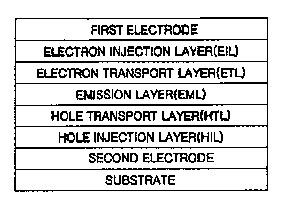
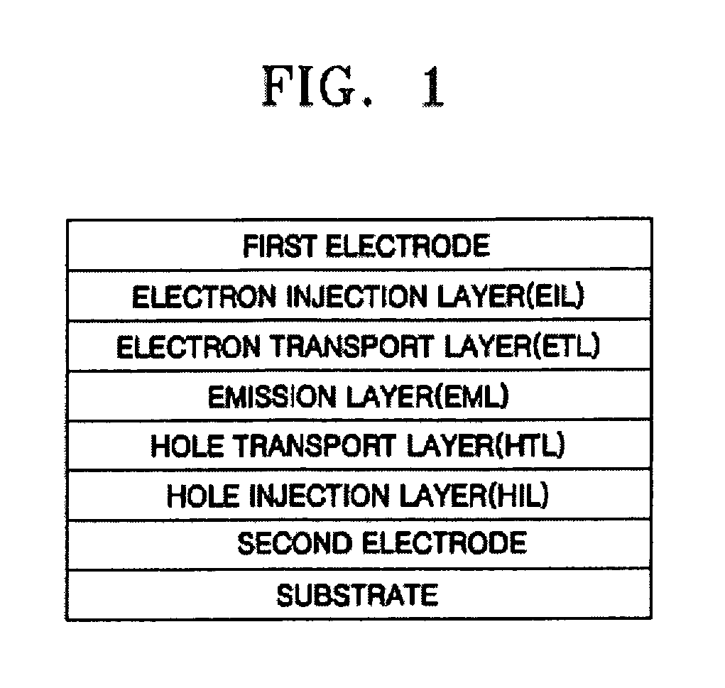
Image

Examples
example 1
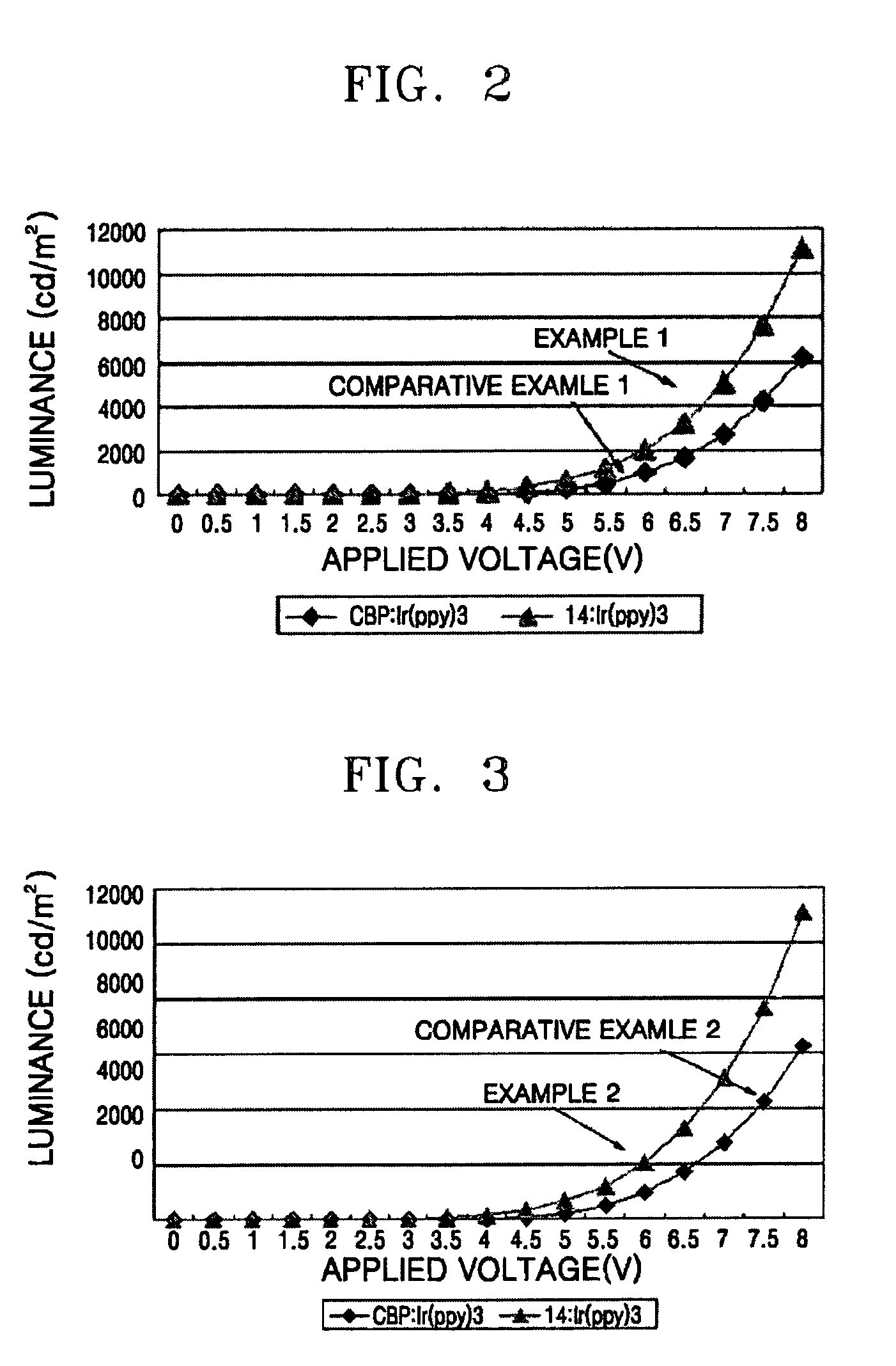
[0088]A ITO glass substrate (Corning Co, surface resistance: 15 Ω / cm2, thickness: 1200 Å) was cut to a size of 50 mm×50 mm×0.7 mm to form an anode. Next the substrate was ultrasonically cleaned in isopropyl alcohol and pure water each for 5 minutes, then irradiated with UV light for 30 minutes, exposed to ozone, and washed. Then, the glass substrate was placed on a vacuum evaporator.
[0089]IDE406 (available from Idemitsu) was vacuum evaporated on the glass is substrate to form an HIL having a thickness of 600 Å. Then, 4,4′-bis[N-(1-naphthyl)-N-phenylaamino]biphenyl (NPB) was vacuum evaporated to a thickness of 300 Å on the HIL to form an HTL.
[0090]Subsequently, a mixture of the compound 14 as a phosphorescent host and Ir(ppy)3 as a green phosphorescent dopant in a weight ratio of 93:7 was deposited on the HTL to form an EML with a thickness of 300 Å. Alq3 was deposited on the EML to form an ETL having a thickness of 300 Å. LiF was deposited on the ETL to form an EIL having a thicknes...
example 2
[0095]A ITO glass substrate (Corning Co, surface resistance: 15 Ω / cm2, thickness: 1200 Å) was cut to a size of 50 mm×50 mm×0.7 mm to form an anode. Next, the substrate was ultrasonically cleaned in isopropyl alcohol and pure water each for 5 minutes, irradiated with UV light for 30 minutes, exposed to ozone, and washed. Then, the glass substrate was placed on a vacuum evaporator. IDE406 was vacuum evaporated on the glass substrate to form an HIL having a thickness of 600 Å. Then, NPB was vacuum evaporated to a thickness of 300 Å on the HIL to form an HTL. Subsequently, a mixture of the compound 14 as a phosphorescent host and RD61 (available from UDC) as a red phosphorescent dopant at a weight ratio of 90:10 was deposited on the HTL to form an EML having a thickness of 300 Å.
[0096]Alq3 was then deposited on the EML to form an ETL with a thickness of 300 Å. LiF was deposited on the ETL to form an EIL having a thickness of 10 Å and Al was deposited on the EIL to form a cathode having ...
PUM
| Property | Measurement | Unit |
|---|---|---|
| internal quantum efficiency | aaaaa | aaaaa |
| internal quantum efficiency | aaaaa | aaaaa |
| internal quantum efficiency | aaaaa | aaaaa |
Abstract
Description
Claims
Application Information