Memory accessing circuit and method

a memory accessing circuit and memory accessing technology, applied in the field can solve the problems of large power consumption and large area of memory accessing circuits, and achieve the effects of reducing the number of impedance paths, increasing the density of memory devices, and reducing circuit area

Active Publication Date: 2010-06-15
IND TECH RES INST
View PDF2 Cites 2 Cited by
  • Summary
  • Abstract
  • Description
  • Claims
  • Application Information

AI Technical Summary

Benefits of technology

[0011]Accordingly, the memory accessing circuit of the present invention is able to reduce the number of impedance paths of the reference circuit by using a median signal generating circuit and a reference signal generating circuit. The circuit area is reduced and the memory unit density of the memory device is increased. Power consumption is also reduced.

Problems solved by technology

Because each reference path is comprised of multiple sets of resistors, more reference paths result in larger area of memory accessing circuits and greater power consumption.

Method used


Image

  • Memory accessing circuit and method
  • Memory accessing circuit and method
  • Memory accessing circuit and method

Examples


Embodiment Construction

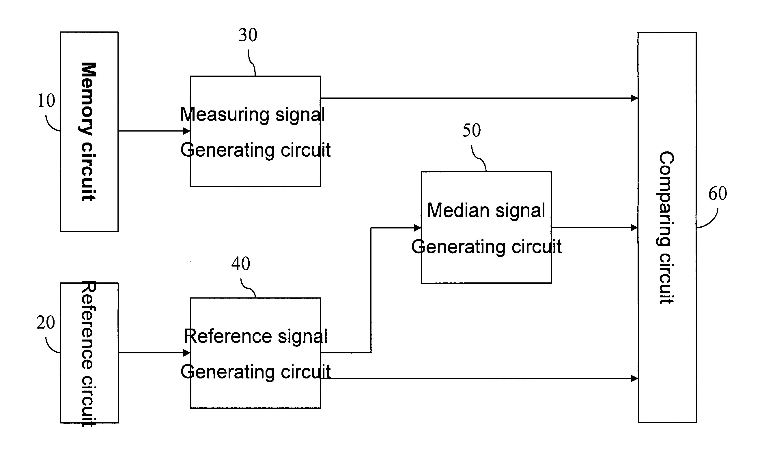
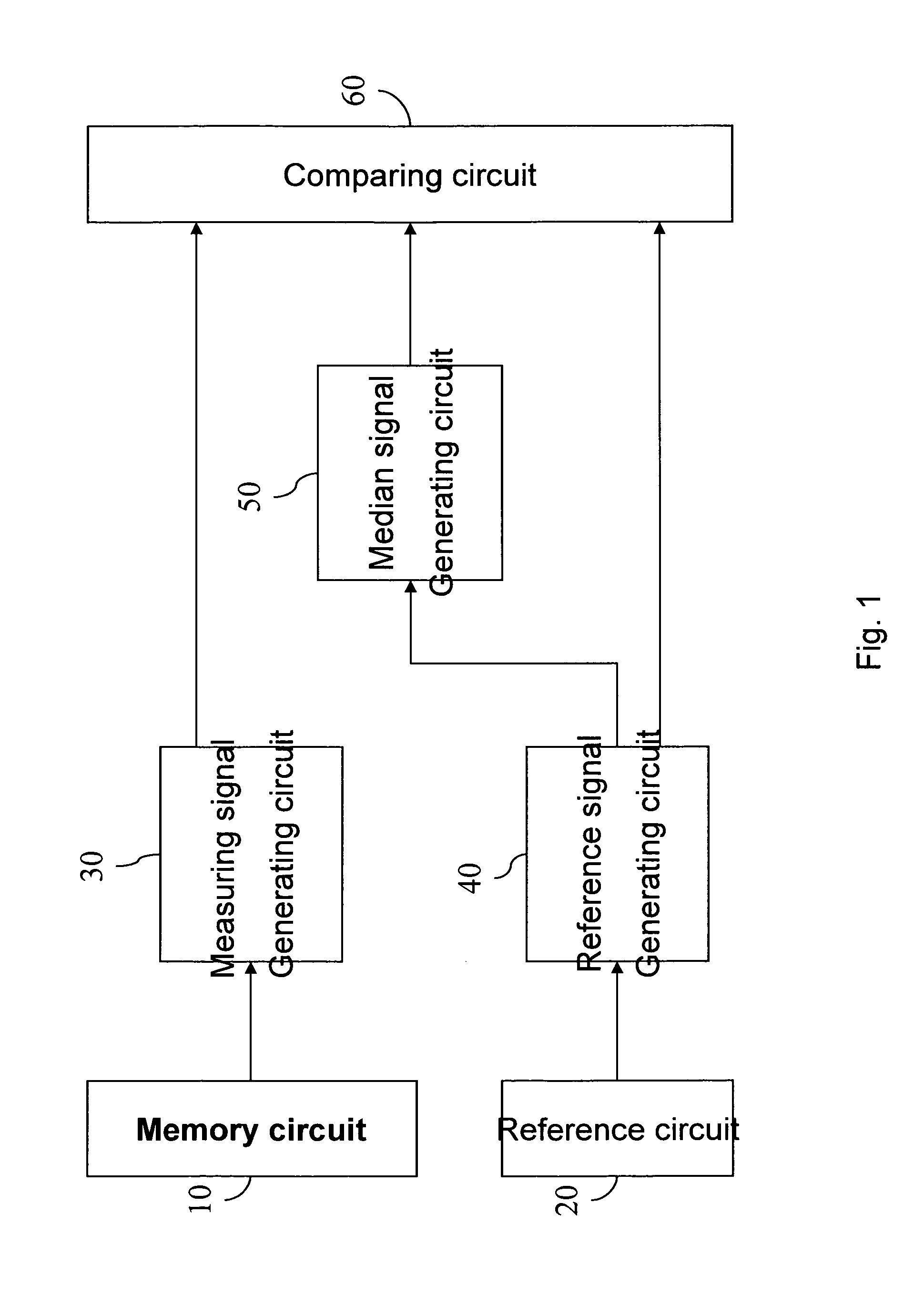
[0021]The present invention discloses a memory accessing circuit and method, which receives an accessing signal from memory cells, compares the accessing signal with a plurality of reference signals generated from a reference circuit and a median signal, and determines the stored state of the memory.

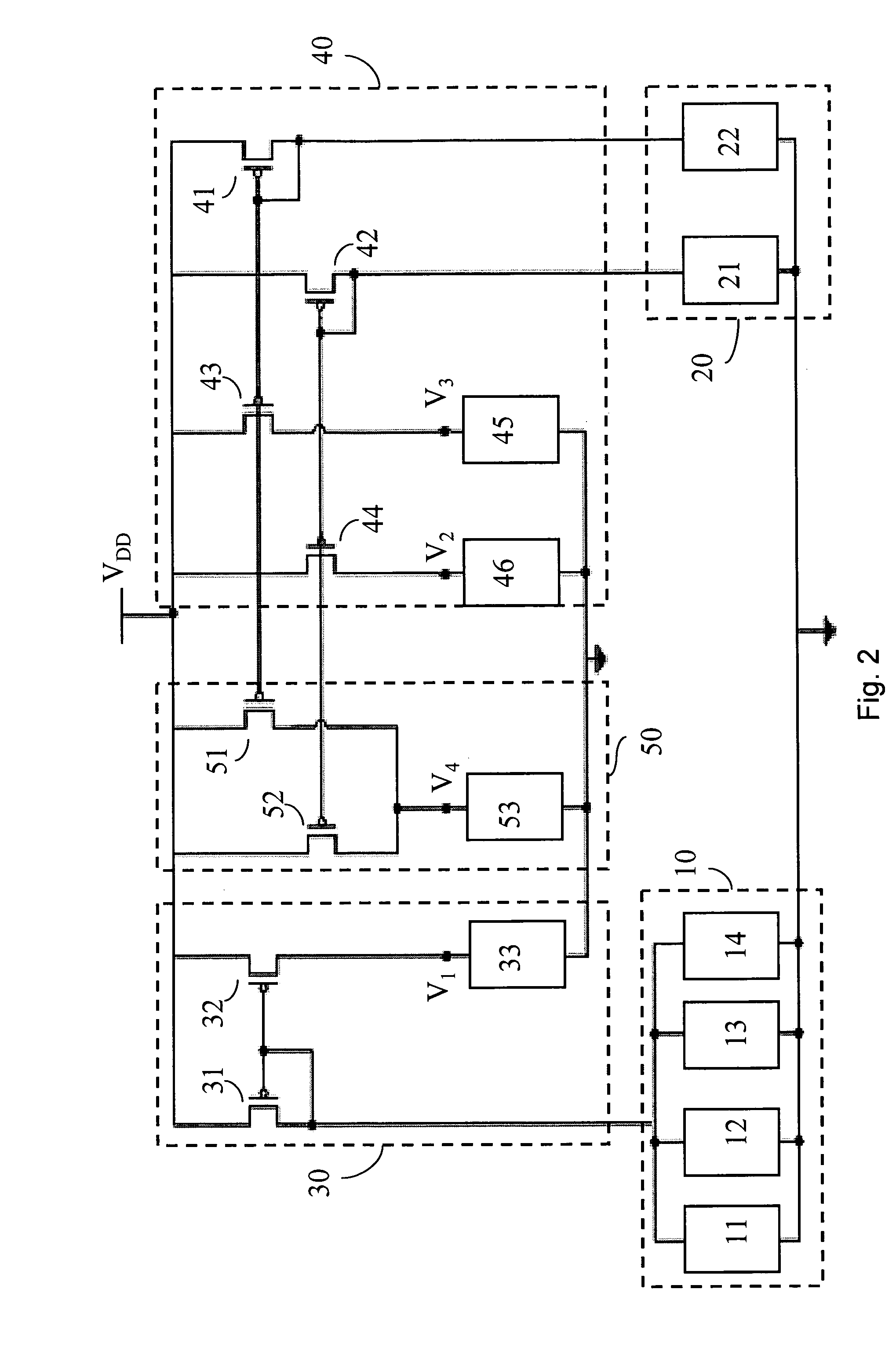
[0022]FIG. 1 is an exemplary memory accessing circuit system schematic. As shown, the memory accessing circuit comprises a memory circuit 10, a reference circuit 20, a testing signal generating circuit 30, a reference signal generating circuit 40, a median signal generating circuit 50, and a comparing circuit 60.

[0023]The memory circuit 10 is a memory cell of a memory and has multiple impedance states. The memory circuit 10 selects one of the impedance states to represent the stored state of the memory. The testing signal generating circuit 30 generates a testing signal according to the impedance state of the memory circuit 10 for determination of the stored state.

[0024]The reference cir...


PUM


Abstract

The present invention relates to a memory accessing circuit, which is for accessing a memory circuit with 2N impedance states. The memory accessing circuit includes a testing signal generating circuit, for generating a testing signal by detecting the impedance state of the memory circuit; a reference signal generating circuit, for generating 2N−1 reference signals by detecting the impedance states of a reference circuit having 2N−1 impedance paths; a median signal generating circuit, for generating (2N−1)−1, median signals by receiving the 2N−1 reference signals; and a comparing circuit, for comparing the testing signal and the (2N−1) median signals. The present invention further provides a memory accessing method thereof.

Description

BACKGROUND OF THE INVENTION[0001]The present invention relates to a memory accessing circuit, especially a multi-state accessing circuit for accessing 4 or more states.[0002]A known magnetic random access memory having 4 states is comprised of one large memory cell and one small memory cell as shown in FIG. 5A. By changing the magnetized polarities of the magnetized memory layers, resistors R1 and R2 can change resistance of the memory cell. Because the logic state of the memory cells having different resistances for 0 and 1, when applying bias to the memory cells, different currents are generated. By determining the value of the currents, the logic state of the memory cells being 0 or 1 can be determined.[0003]Also, memory cell accessing rates are closely related to a sense amplifier. The faster for the sense amplifier determines the state of the memory cell, the better it is. The time it takes to determine the state of the memory cell is also related to the value of the current.[0...

Claims


Application Information

Patent Timeline
Patent Type & Authority Patents(United States)
IPC IPC(8): G11C11/00
CPCG11C29/08G11C11/5607G11C11/16G11C2211/5634
Inventor WANG, MIN CHUANLIN, CHIH SHENGSU, KENG LICHANG, WEI CHUN
Owner IND TECH RES INST
Why Eureka
Try Eureka