Method of forming a FET having ultra-low on-resistance and low gate charge

a transistor and gate charge technology, applied in the field of field effect transistors, can solve the problems of reducing the switching capability of the device, affecting the reproducibility of the device having desired performance capabilities, and limiting certain performance characteristics of the transistor, so as to achieve low gate charge, reduce the variation of transistor characteristics, and reduce the effect of resistance rds

Inactive Publication Date: 2010-06-29
SEMICON COMPONENTS IND LLC
View PDF298 Cites 18 Cited by
  • Summary
  • Abstract
  • Description
  • Claims
  • Application Information

AI Technical Summary

Benefits of technology

[0009]In accordance with the present invention, a trench DMOS transistor is characterized by an ultra-low on resistance RDS(on) and a low gate charge. The structure and method of manufacturing the DMOS transistor minimizes variations in the transistor characteristics by controlling substrate out-diffusion.
[0014]In another embodiment, during the one or more temperature cycles the substrate cap region influences said out-diffusion of the dopants of the first conductivity type into the body region such that the length of the channel region varies less and thus is substantially predictable.

Problems solved by technology

A high RDS(on) limits certain performance characteristics of the transistor.
The higher Qg is the larger the gate-to-drain overlap capacitance becomes and, consequently, the lower the switching capability of the device becomes.
Wide device-to-device variations negatively affect the reproducibility of a device having desired performance capabilities.

Method used


Image

  • Method of forming a FET having ultra-low on-resistance and low gate charge
  • Method of forming a FET having ultra-low on-resistance and low gate charge
  • Method of forming a FET having ultra-low on-resistance and low gate charge

Examples


Embodiment Construction

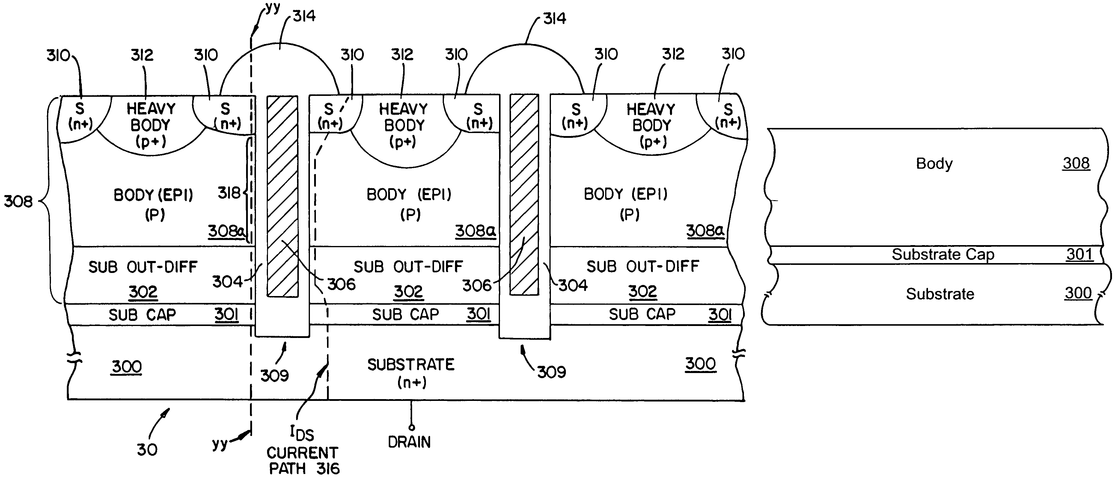
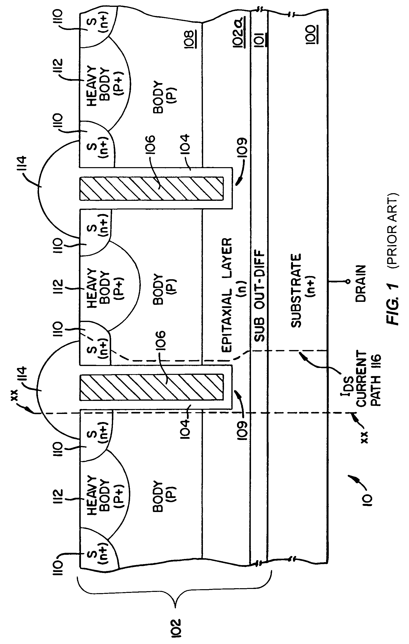
[0027]The present invention is directed to a trench MOSFET device, and its method of manufacture, that can be used in applications such as cellular phone power supplies and battery switching. The trench MOSFET of the present invention is defined by a structure having a low drain-to-source resistance, low gate charge and a method of fabrication that minimizes device-to-device variations in operating characteristics by controlling out-diffusion from the transistor substrate.

[0028]FIG. 3 shows a cross-sectional illustration of an exemplary n-channel trench DMOS transistor 30 according to one embodiment of the present invention. Trench DMOS transistor 30 includes an n-type substrate 300, which has a resistivity of, for example, 1-5 mΩ-cm, over which a substrate cap region 301 is formed. Substrate cap region 301 is heavily doped and has a resistivity of, for example, 1 mΩ-cm. Substrate cap region 301 functions to provide a more constant resistivity range than what substrate vendors typic...


PUM


Abstract

In accordance with an exemplary embodiment of the invention, a substrate of a first conductivity type silicon is provided. A substrate cap region of the first conductivity type silicon is formed such that a junction is formed between the substrate cap region and the substrate. A body region of a second conductivity type silicon is formed such that a junction is formed between the body region and the substrate cap region. A trench extending through at least the body region is then formed. A source region of the first conductivity type is then formed in an upper portion of the body region. An out-diffusion region of the first conductivity type is formed in a lower portion of the body region as a result of one or more temperature cycles such that a spacing between the source region and the out-diffusion region defines a channel length of the field effect transistor.

Description

CROSS-REFERENCES TO RELATED APPLICATIONS[0001]This application is a continuation-in-part of U.S. application Ser. No. 10 / 754,276, filed Jan. 8, 2004, which is a divisional of U.S. application Ser. No. 09 / 640,955, filed Aug. 16, 2000, now U.S. Pat. No. 6,696,726, entitled “Vertical MOSFET with Ultra-low Resistance and Low Gate Charge”, which disclosures are incorporated herein by reference in their entirety.[0002]Two other related patents are U.S. Pat. No. 6,437,386, entitled “Method for Creating Thick Oxide on the Bottom Surface of a Trench Structure in Silicon” and U.S. Pat. No. 6,444,528, entitled “Selective Oxide Deposition in the Bottom of a Trench,” both of which are assigned to the present assignee and are incorporated herein by reference for all purposes.BACKGROUND OF THE INVENTION[0003]The present invention relates to field effect transistors (FETs) and, in particular, to trench metal-oxide-semiconductor (MOS) transistors and methods of fabricating the same.[0004]Power Metal...

Claims


Application Information

Patent Timeline
Patent Type & Authority Patents(United States)
IPC IPC(8): H01L21/336H01L29/08H01L29/423H01L29/78
CPCH01L29/7813H01L29/0847H01L29/42368H01L29/0878H01L29/66734H01L29/1095
Inventor BENCUYA, IZAKMO, BRIAN SZE-KICHALLA, ASHOK
Owner SEMICON COMPONENTS IND LLC
Why Eureka
Try Eureka