
Memory comprising diode

a memory cell and diode technology, applied in the field of memory, can solve the problems of disadvantageous difficulty in operating the diode rom at a high speed, and achieve the effect of inhibiting the selection of bit lines from potential fluctuation and high speed

Inactive Publication Date: 2010-06-29
SEMICON COMPONENTS IND LLC
View PDF6 Cites 2 Cited by
  • Summary
  • Abstract
  • Description
  • Claims
  • Application Information

AI Technical Summary

Benefits of technology

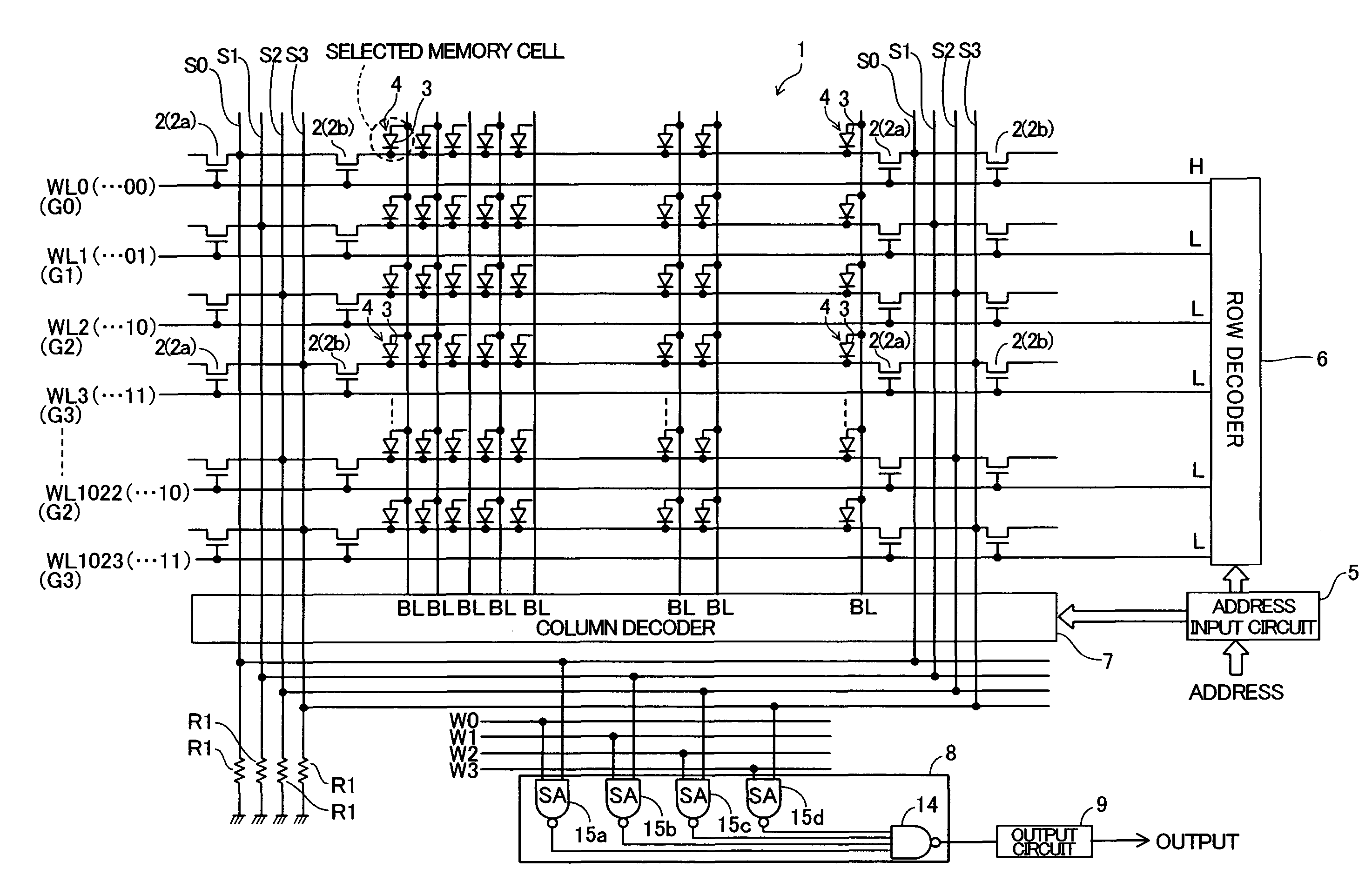
The present invention provides a memory that operates at high speed. The memory includes a plurality of word lines, first transistors, memory cells, and a data determination portion. The cathodes of the diodes in the memory cells are connected to the first transistors, and the data determination portion is connected to the drain or source regions of the first transistors for determining data from the selected memory cell. This allows the memory to determine data based on the potentials of the drain or source regions of the first transistors without connecting the bit lines to the data determination portion. The memory can fix a selected bit line to a first potential and a non-selected bit line to a second potential, preventing potential fluctuation and ensuring high-speed operation.

Problems solved by technology

Thus, it is disadvantageously difficult to operate the diode ROM at a high speed.

Method used


Image

  • Memory comprising diode
  • Memory comprising diode
  • Memory comprising diode

Examples


first embodiment

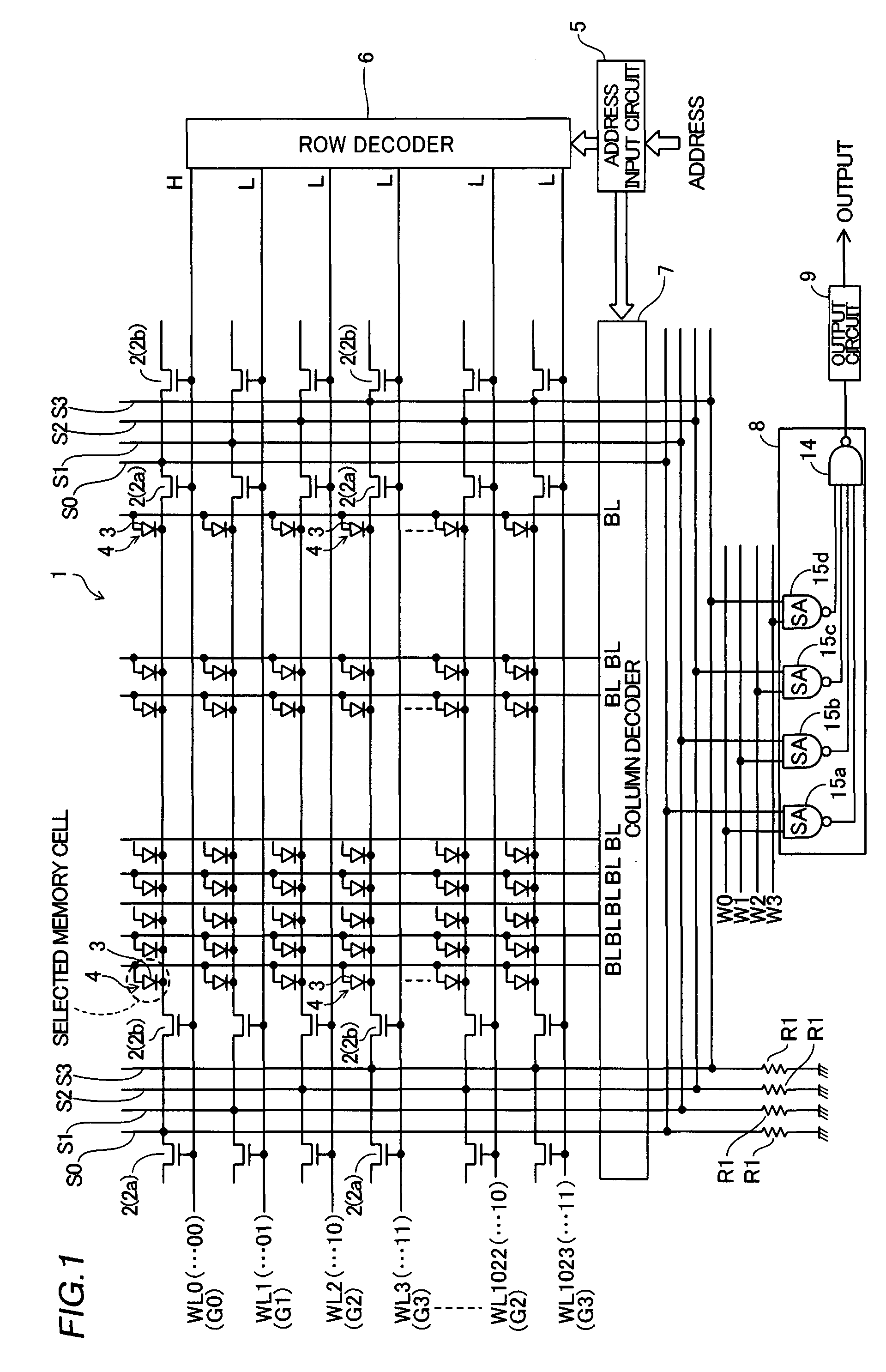
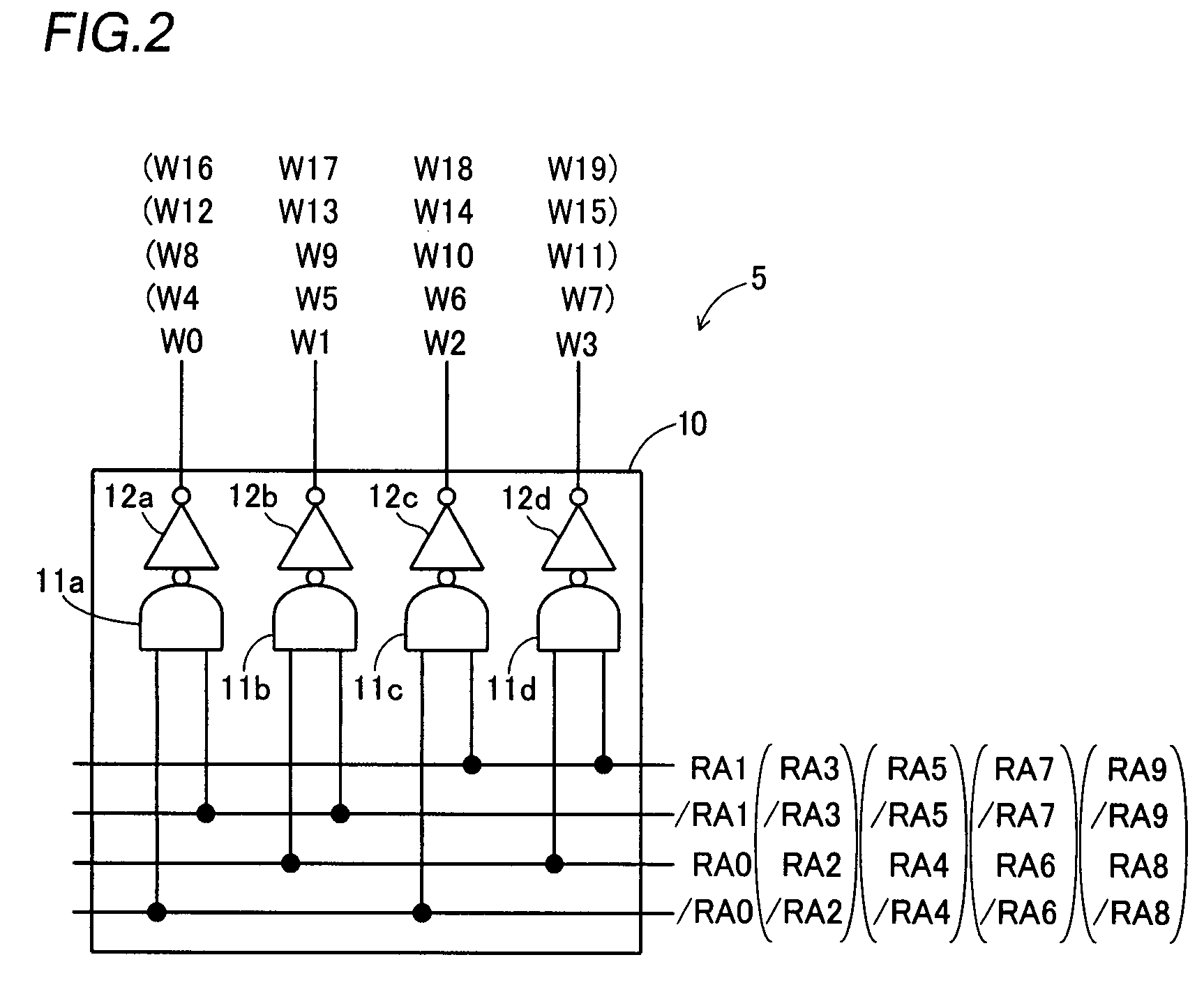
[0029]The structure of a crosspoint diode ROM according to a first embodiment of the present invention is described with reference to FIGS. 1 to 3.

[0030]In the crosspoint diode ROM according to the first embodiment, a plurality of word lines WL and a plurality of bit lines BL are arranged in a memory cell array 1 to intersect with each other, as shown in FIG. 1. The word lines WL and the bit lines BL are connected to a row decoder 6 and a column decoder 7 respectively, as described later. According to the first embodiment, 1024 word lines WL are arranged in the memory cell array 1, and an address having a plurality of digits consisting of bits including “0” and “1” is allocated to each of the 1024 word lines WL. While serial numbers 0 to 1023 are sequentially assigned to the 1024 word lines WL, FIG. 1 illustrates only the word lines WL having the serial numbers 0 to 3, 1022 and 1023.

[0031]According to the first embodiment, the 1024 word lines WL are classified into four word line gr...

second embodiment

[0060]Referring to FIGS. 4 to 6, 1024 word lines WL are classified into 16 word line groups G0 to G15 in a crosspoint diode ROM according to a second embodiment of the present invention, dissimilarly to the aforementioned first embodiment.

[0061]In the crosspoint diode ROM according to the second embodiment, a plurality of (1024) word lines WL and a plurality of bit lines BL are arranged in a memory cell array 21 to intersect with each other similarly to the aforementioned first embodiment, as shown in FIG. 4. FIG. 4 illustrates only word lines WL having serial numbers 0, 1, 63, 64, 1020 and 1023 included in the 1024 word lines WL.

[0062]According to the second embodiment, the 1024 word lines WL are classified into the 16 word lie groups G0 to G15 each including 64 word lines WL. More specifically, the first word line group G0 includes the first to 64th word lines WL0 to WL63, and the second word line group G1 includes the 65th to 128th word lines WL64 to WL127. The word line groups G...

third embodiment

[0090]Referring to FIGS. 7 to 10, a crosspoint diode ROM according to a third embodiment of the present invention includes a word line control circuit 66, dissimilarly to the aforementioned first embodiment.

[0091]In the diode ROM according to the third embodiment, a plurality of word lines WL and a plurality of bit lines BL are arranged in a memory cell array 61 to intersect with each other similarly to the aforementioned first embodiment, as shown in FIG. 7. FIG. 7 illustrates only the word lines WL having serial numbers 0 to 3, 1020 and 1023 included in 1024 word lines WL.

[0092]The 1024 word lines WL are classified into four word line groups G0 to G3 each including 256 word lines WL, similarly to the aforementioned first embodiment. The gate electrodes of a prescribed number of selection transistors 62 are connected to each word line WL at prescribed intervals. The selection transistors 62 are similar in structure to the selection transistors 2 according to the aforementioned firs...


PUM


Abstract

A memory operable at a high speed is obtained. This memory comprises a plurality of word lines, first transistors each connected to each the plurality of word lines for entering an ON-state through selection of the corresponding word line, a plurality of memory cells including diodes having cathodes connected to the source or drain regions of the first transistors respectively and a data determination portion connected to the drain or source regions of the first transistors for determining data read from a selected memory cell.

Description

BACKGROUND OF THE INVENTION[0001]1. Field of the Invention[0002]The present invention relates to a memory, and more particularly, it relates to a memory comprising memory cells including diodes.[0003]2. Description of the Background Art[0004]Japanese Patent Laying-Open No. 2005-268370 discloses a crosspoint mask ROM (hereinafter referred to as a crosspoint diode ROM) having a plurality of memory cells, each including a diode, arranged in the form of a matrix. This crosspoint diode ROM is generally known as an exemplary memory.[0005]FIG. 11 is a circuit diagram showing the structure of the conventional crosspoint diode ROM disclosed in the aforementioned Japanese Patent Laying-Open No. 2005-268370. Referring to FIG. 11, a plurality of word lines WL and a plurality of bit lines BL are arranged in a memory cell array 101 to intersect with each other in the conventional crosspoint diode ROM. The word lines WL and the bit lines BL are connected to a row decoder 106 and a column decoder 1...

Claims


Application Information

Patent Timeline
Patent Type & Authority Patents(United States)
IPC IPC(8): G11C11/36
CPCG11C17/10
Inventor YAMADA, KOUICHI
Owner SEMICON COMPONENTS IND LLC
Learn More