Intermediate-band photosensitive device with quantum dots embedded in energy fence barrier

a photosensitive device and quantum dots technology, applied in the field of photosensitive optoelectronic devices, can solve the problems of poor carrier mobility of insulations

Active Publication Date: 2010-07-06
THE TRUSTEES FOR PRINCETON UNIV
View PDF13 Cites 38 Cited by
  • Summary
  • Abstract
  • Description
  • Claims
  • Application Information

AI Technical Summary

Problems solved by technology

In comparison to semiconductors, insulators generally provide poor carrier mobility.

Method used


Image

  • Intermediate-band photosensitive device with quantum dots embedded in energy fence barrier
  • Intermediate-band photosensitive device with quantum dots embedded in energy fence barrier
  • Intermediate-band photosensitive device with quantum dots embedded in energy fence barrier

Examples


Embodiment Construction

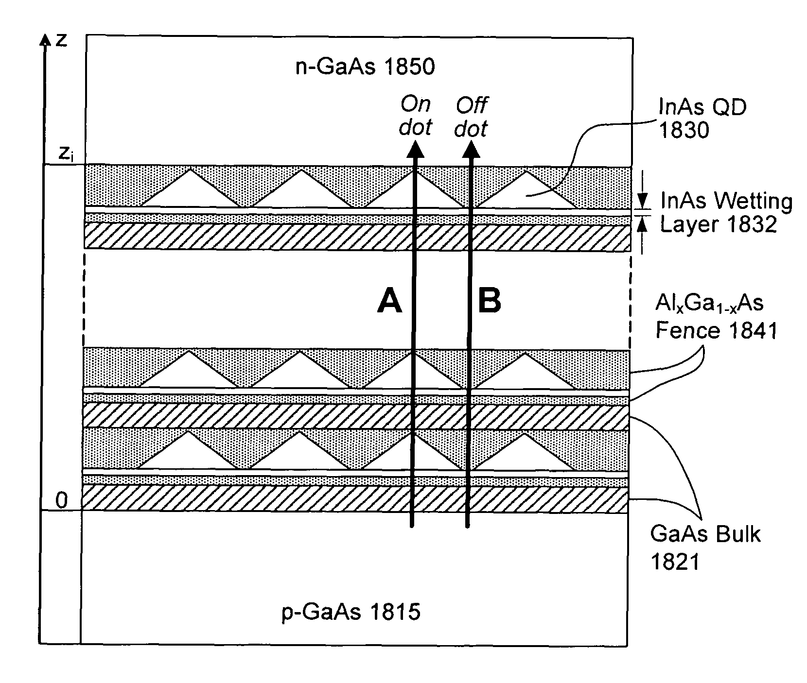
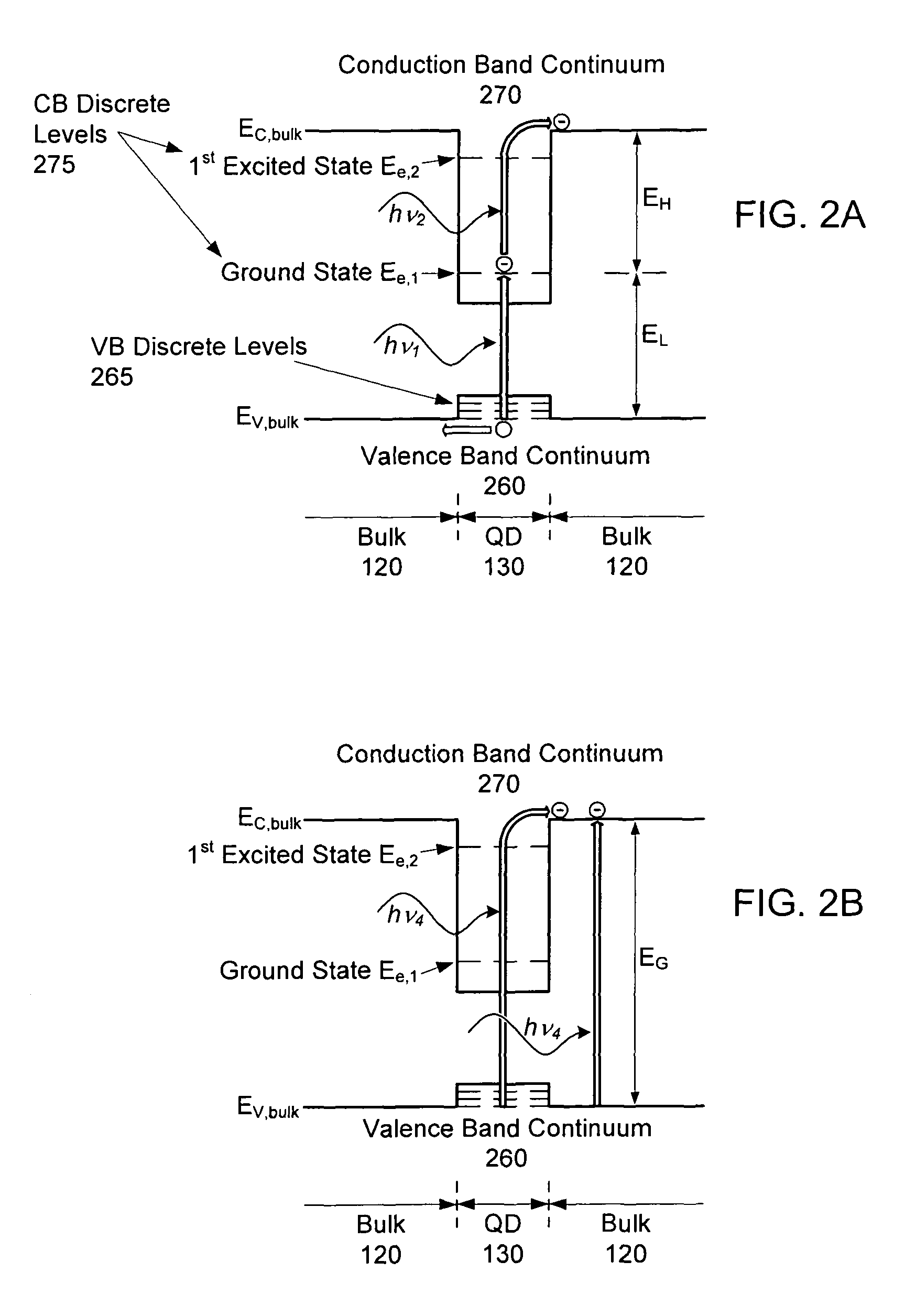
[0056]One method being explored to improve the efficiency of solar cells is to use quantum dots to create an intermediate band within the bandgap of the solar cell. Quantum dots confine charge carriers (electrons, holes, and / or excitons) in three-dimensions to discrete quantum energy states. The cross-sectional dimension of each quantum dot is typically on the order of hundreds of Ångstroms or smaller. An intermediate-band structure is distinguishable, among other ways, by the overlapping wave functions between dots. The “intermediate” band is the continuous miniband formed by the overlapping wave functions. Although the wave functions overlap, there is no physical contact between adjacent dots.

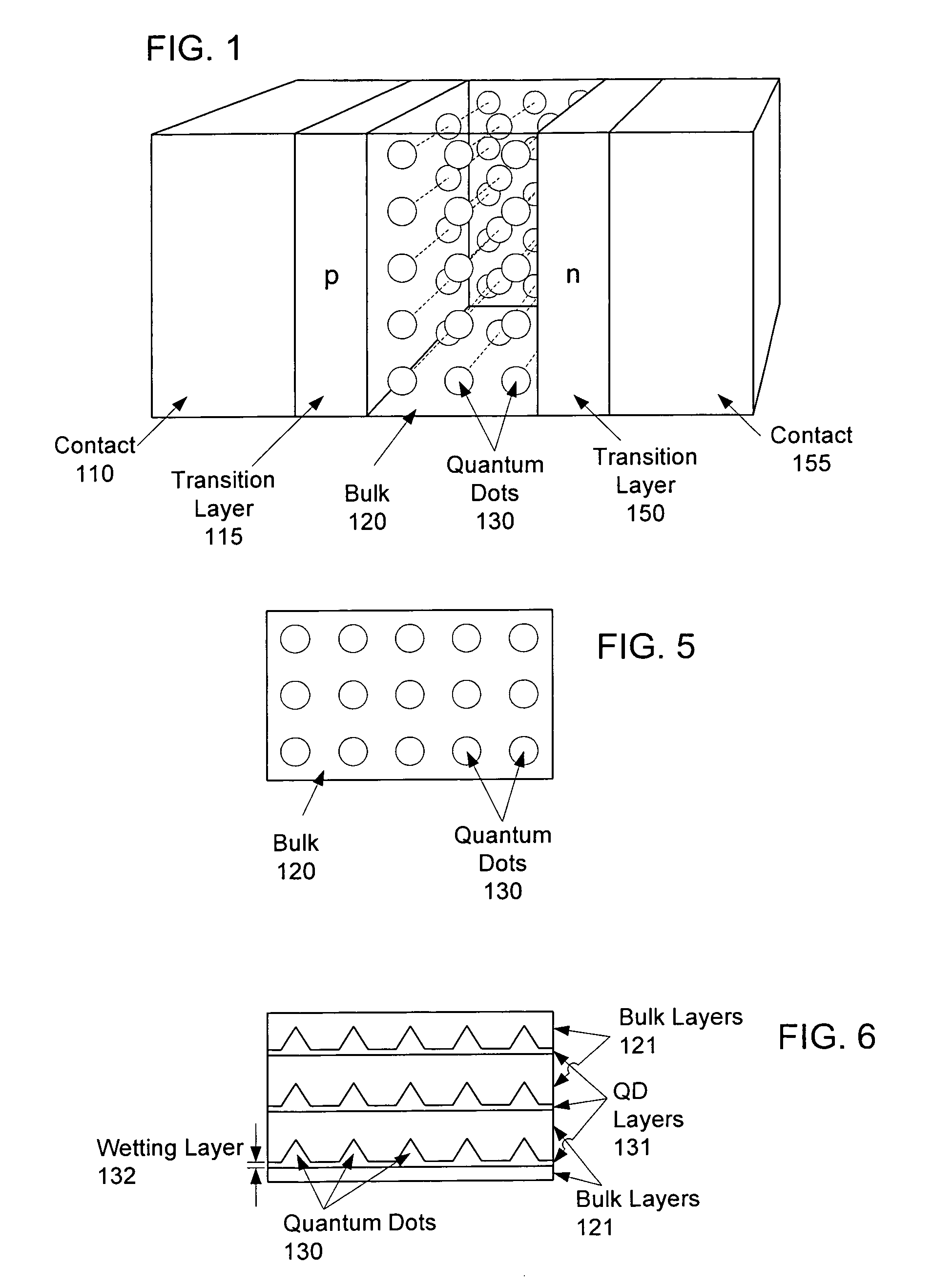
[0057]FIG. 1 illustrates an example of an intermediate-band device. The device comprises a first contact 110, a first transition layer 115, a plurality of quantum dots 130 embedded in a semiconductor bulk matrix material 120, a second transition layer 150, and a second contact 155.

[0058]In a ...


PUM


Abstract

A plurality of layers of a first semiconductor material and a plurality of dots-in-a-fence barriers disposed in a stack between a first electrode and a second electrode. Each dots-in-a-fence barrier consists essentially of a plurality of quantum dots of a second semiconductor material embedded between and in direct contact with two layers of a third semiconductor material. Wave functions of the quantum dots overlap as at least one intermediate band. The layers of the third semiconductor material are arranged as tunneling barriers to require a first electron and / or a first hole in a layer of the first material to perform quantum mechanical tunneling to reach the second material within a respective quantum dot, and to require a second electron and / or a second hole in a layer of the first semiconductor material to perform quantum mechanical tunneling to reach another layer of the first semiconductor material.

Description

RELATED APPLICATIONS[0001]This application is a continuation-in-part of U.S. application Ser. No. 11 / 304,713 filed Dec. 16, 2005 (pending), the contents of which are incorporated herein by reference.UNITED STATES GOVERNMENT RIGHTS[0002]This invention was made with government support under Contract No. XAT-5-33636-03 awarded by the U.S. Department of Energy, National Renewable Energy Laboratory. The government has certain rights in the invention.JOINT RESEARCH AGREEMENT[0003]Portions of the claimed invention were made by, on behalf of, and / or in connection with one or more of the following parties to a joint university-corporation research agreement Princeton University, The University of Southern California, and Global Photonic Energy Corporation. The remainder of the claimed invention was made by, on behalf of, and / or in connection with one or more of the following parties to a joint university-corporation research agreement. The University of Michigan, The University of Southern C...

Claims


Application Information

Patent Timeline
Patent Type & Authority Patents(United States)
IPC IPC(8): H01L27/14
CPCB82Y10/00B82Y15/00B82Y20/00H01L31/09H01L31/18H01L31/035236Y02E10/544Y02E10/50H01L31/042
Inventor FORREST, STEPHEN R.WEI, GUODAN
Owner THE TRUSTEES FOR PRINCETON UNIV
Why Eureka
Try Eureka