Lead-on-chip semiconductor package and leadframe for the package

a technology of leadframe and semiconductor package, which is applied in the direction of semiconductor devices, semiconductor/solid-state device details, electrical apparatus, etc., can solve the problems of delamination or breakage, short electrical circuit, etc., and achieve the effect of reducing the possibility of dummy finger delamination, reducing the possibility of shifting nor tilting, and improving the product reliability of loc semiconductor packag

Inactive Publication Date: 2010-07-06
POWERTECH TECHNOLOGY INC
View PDF2 Cites 1 Cited by
  • Summary
  • Abstract
  • Description
  • Claims
  • Application Information

AI Technical Summary

Benefits of technology

[0004]The main purpose of the present invention is to provide a LOC semiconductor package to reduce the stresses concentrated on some bonding fingers of the leads located at two corresponding far edges along the bonding fingers to eliminate the electrical short between the delaminated bonding fingers and the adjacent bonding fingers.
[0005]The second purpose of the present invention is to provide a LOC semiconductor package to dispose dummy finger without any electrical connections at two corresponding far edges along the bonding fingers to bear thermal stresses so that the electrical functions of the LOC semiconductor package will not be impacted even if the dummy finger are delaminated or even broken.
[0006]The third purpose of the present invention is to provide a LOC semiconductor package to enhance the stress resistance of the dummy finger.

Problems solved by technology

Since the CTE of the leadframe is different from the one of the chip, the thermal stresses induced by the thermal cycles during die-attaching processes and molding processes will be concentrated at certain leads, especially at the leads adjacent to the chip edges, leading to delamination or broken leads.
Moreover, the delaminated bonding fingers 111A even contact with the adjacent bonding fingers 111 during molding processes leading to electrically short.

Method used


Image

  • Lead-on-chip semiconductor package and leadframe for the package
  • Lead-on-chip semiconductor package and leadframe for the package
  • Lead-on-chip semiconductor package and leadframe for the package

Examples


Embodiment Construction

[0021]Please refer to the attached drawings, the present invention will be described by means of embodiments below.

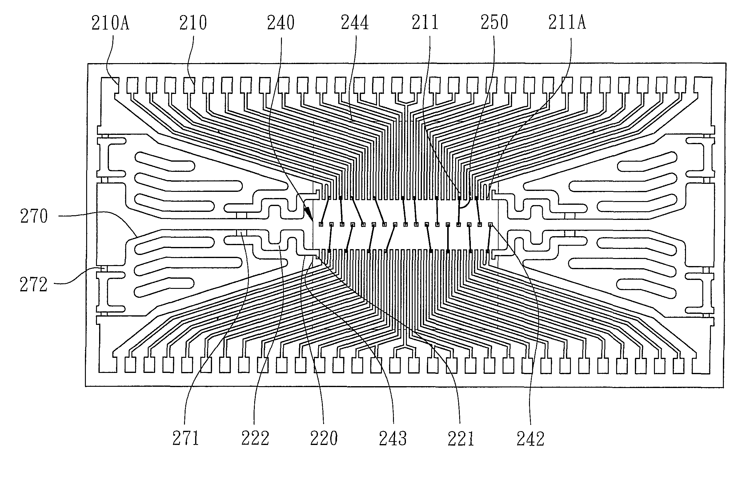
[0022]According to the first embodiment of the present invention, as shown in FIG. 4, a LOC semiconductor package 200 primarily comprises a plurality of leadframe's leads 210, at least a tie bar 220, a die-attaching layer 230, a chip 240, a plurality of bonding wires 250, and an encapsulant 260. As shown in FIG. 5, the leads 210 and the tie bar 220 are formed from the same metal leadframe with a thickness of about 0.2 mm to provide enough structural strength to support the chip 240. Each lead 210 has a bonding finger 211 at the internal end of the lead 210. As shown in FIG. 5 again, without limitations, the leads 210 can be arranged at two opposing longer sides of a leadframe in a packaging unit where the internal ends of the leads 210 are extended toward the center in a fan-in design through the encapsulation area of the encapsulant 260 and a die-attaching area 201 (th...


PUM


Abstract

A LOC semiconductor package with the leadframe for the package is revealed. The LOC semiconductor package primarily comprises a plurality of leadframe's leads, at least a tie bar, a chip, and an encapsulant encapsulating the components mentioned above. Each lead has a bonding finger. The tie bar has a dummy finger where the dummy finger is linearly disposed at one side of the disposition area of the bonding fingers. The chip has an active surface with the bonding fingers. When the dummy finger and the bonding fingers are disposed above the active surface by a die-attaching layer, the dummy finger is adjacent to one edge of the active surface. The bonding fingers are electrically connected with the bonding pads. The dummy finger will bear the concentrated stresses to avoid the bonding fingers on the active surface to delamination or break due to external stresses and to avoid the interference to the layout of the leads.

Description

FIELD OF THE INVENTION[0001]The present invention relates to semiconductor devices, especially to Lead-On-Chip (LOC) semiconductor packages.BACKGROUND OF THE INVENTION[0002]Conventionally, a LOC (Lead-On-Chip) semiconductor package includes a semiconductor chip encapsulated by an encapsulant to prevent the contaminations of dust particles and moisture and a plurality of leads of a leadframe carrying the chip and transmitting the electrical signals of the chip to external electrical components. “Lead-On-Chip” means the leads of the leadframe are extended to the active surface of a chip with the chip attached to the leads of a leadframe to eliminate or minimize die pad(s). Since the CTE of the leadframe is different from the one of the chip, the thermal stresses induced by the thermal cycles during die-attaching processes and molding processes will be concentrated at certain leads, especially at the leads adjacent to the chip edges, leading to delamination or broken leads.[0003]As sho...

Claims


Application Information

Patent Timeline
Patent Type & Authority Patents(United States)
IPC IPC(8): H01L23/495
CPCH01L23/4951H01L2224/48091H01L2224/48247H01L2224/4826H01L2924/00014H01L24/48H01L2224/32245H01L2224/73215H01L2924/00H01L2924/181H01L2224/05554H01L2224/45099H01L2224/45015H01L2924/207H01L2924/00012
Inventor FAN, WEN-JENGHSU, YU-MEI
Owner POWERTECH TECHNOLOGY INC
Why Eureka
Try Eureka