High speed CMOS output buffer for nonvolatile memory devices

a memory device and output buffer technology, applied in logic circuits, power consumption reduction, electric pulse generators, etc., can solve the problems of buffer not meeting the above mentioned requirements, complex transmission, and increasing circuit complexity, so as to reduce or minimize the contribution to power consumption

Active Publication Date: 2010-07-06
STMICROELECTRONICS SRL
View PDF3 Cites 3 Cited by
  • Summary
  • Abstract
  • Description
  • Claims
  • Application Information

AI Technical Summary

Benefits of technology

[0012]An effective way has been found for significantly eliminating or reducing limitations and inefficiencies in realizing a CMOS output buffer for high speed digital applications based on the use of natural complementary transistors, that is transistors with a threshold smaller than the threshold of commonly used enhancement transistors, connected in parallel to transistors of opposite type of conductivity of the complementary enhancement transistor pairs that compose the final inverter stage of the buffer.
[0016]To reduce or minimize the contribution to power consumption due to the bias currents of the respective natural PMOS and NMOS transistors absorbed from the respective boosted voltage sources, the two voltages are generated by the use of respective current mirrors insensitive to variations of the supply voltage of the circuit, to temperature and to process “spread”, the voltages are held by hold capacitors connected between the supply node of the drivers of the two complementary natural transistors connected in parallel to the enhancement transistors of the output stage of the buffer, and to ground, in one case, and to the supply node of the buffer in the other case. And the control gates of the two natural PMOS and NMOS transistors of the two generators of the two voltages are controlled by a stand-by signal of the integrated system to which the output buffer belongs, such to implement a time-division biasing.

Problems solved by technology

Therefore, the line must be properly matched, at least at one end thereof, otherwise signals sent on the line will be reflected to some extent and make transmissions complicated.
This buffer does not satisfy the above mentioned requirements because its output impedance is too large compared to typical values of the characteristic line impedance Z0, as far as the output transistors operate in the saturation region.
The problem is generally overcome by boosting the driving signals of the gates of the added complementary MOS, even if this implies a significant increase of circuit complexity and an increased silicon area overhead (pump capacitors), the amount of which is comparable with the silicon area occupied by the output MOS transistor.
Such a large power consumption could make it difficult to satisfy the power consumption specifications in stand-by when the output buffers are active (i.e. not in tristate condition).
Besides for meeting response speed specifications, the power consumption of the above-mentioned feedback circuit is due to the need of ensuring an adequate overdrive Vgs-Vth to the driver (it must remain turned on), especially if the driver must deliver the current Ioh (or Iol).
Moreover, from the characteristics depicted in FIG. 2, it is evident that, in the linear functioning region of the characteristics, the common source MOS has a smaller output resistance than the required resistance, thus the drivers are over-sized, with a larger silicon area consumption.

Method used


Image

  • High speed CMOS output buffer for nonvolatile memory devices
  • High speed CMOS output buffer for nonvolatile memory devices
  • High speed CMOS output buffer for nonvolatile memory devices

Examples


Embodiment Construction

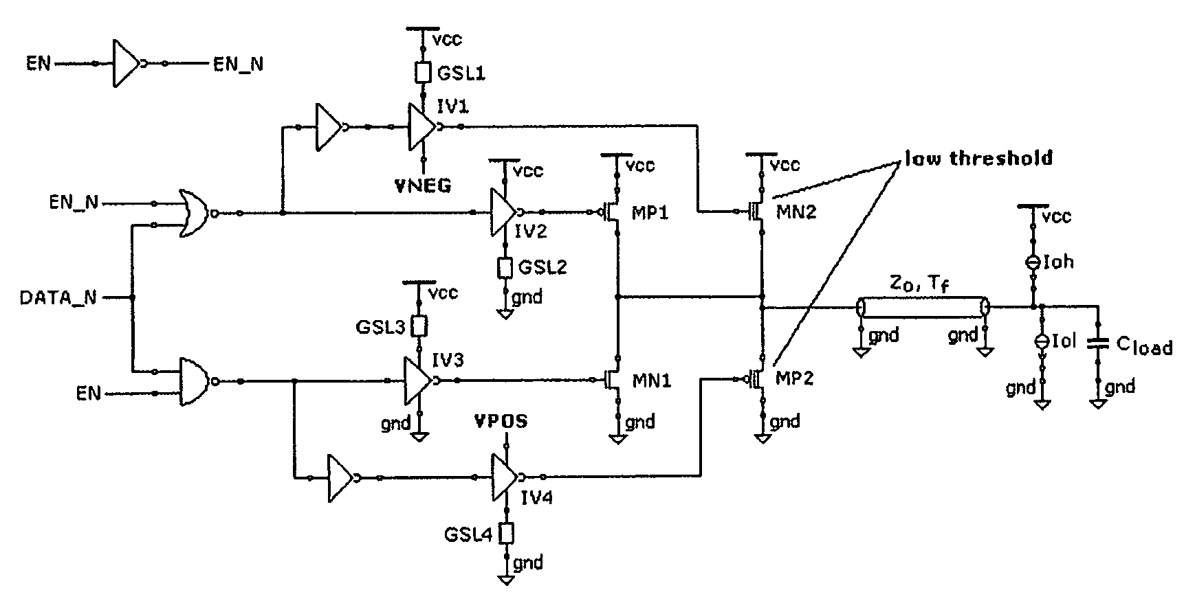
[0026]FIG. 4 depicts a basic circuit diagram of an output buffer according to the invention. The natural MOS transistors are MN2, MP2, and the supply terminals of the inverters IV1 and IV4, not connected to the gate slew limiters for controlling the slope of the gate signals of the output drivers (that is the slope of the variation of the gate voltage) (GSL) that are not directly grounded or connected at the voltage Vcc, but to the supply nodes VNEG and VPOS, respectively.

[0027]In commanded stand-by conditions, or in self-stand-by conditions, VNEG is negative and its absolute value is relatively small, VPOS is positive and slightly higher than Vcc. The voltages VPOS and VNEG are used for preventing circulation of the under-threshold current through the “low threshold” MOS. These transistors are relatively large and the under-threshold current that flows therethrough may become relatively large and may become uncontrolled because of process spreads, supply fluctuations and temperatur...


PUM

PropertyMeasurementUnit
output resistanceaaaaaaaaaa
conductivityaaaaaaaaaa
threshold voltageaaaaaaaaaa

Abstract

An output CMOS buffer includes MOS enhancement transistors and has a second complementary pair of natural or low threshold transistors, connected respectively in parallel to transistors of opposite type of conductivity of the complementary pair of enhancement MOS transistors of the final buffer stage. The gate terminals of the pair of natural or low threshold transistors are controlled by respective inverters, each supplied through a slew rate limiter of the slope of the driving current and are respectively connected between the positive supply node of the output buffer and a negative (below ground potential) node and between the common ground node of the output buffer and a positive supply node. The negative voltage and the positive voltage on the nodes are at least equal to the absolute value of the threshold voltage of the natural or low threshold transistors.

Description

FIELD OF THE INVENTION[0001]The invention relates to high-speed CMOS output buffers, particularly for memory devices.BACKGROUND OF THE INVENTION[0002]When lines of interconnection between two circuits are relatively long or the circuits sufficiently fast such that the rise / fall times of signals exchanged between the circuits are comparable with propagation times over the connection line, then interconnection lines must be treated as long transmission lines. Therefore, the line must be properly matched, at least at one end thereof, otherwise signals sent on the line will be reflected to some extent and make transmissions complicated. Impedance mismatchings may be accepted as far as the consequent increase of the time required for reaching steady-state conditions remains inconsequential.[0003]In CMOS buffers, the more convenient matching is carried out at the input end of the line (null DC power consumption), that is, making the output impedance Zout of the line driving buffer equal t...

Claims


Application Information

Patent Timeline
Patent Type & Authority Patents(United States)
IPC IPC(8): H03B1/00H03K3/00
CPCG11C7/1051G11C7/1057H03K19/0013H03K19/018571H03K19/09429H03K19/01721Y10T29/49117
Inventor LA PLACA, MICHELEMARTINES, IGNAZIO
Owner STMICROELECTRONICS SRL
Why Eureka
Try Eureka