
Method for manufacturing semiconductor device

a semiconductor and manufacturing technology, applied in semiconductor devices, instruments, computing, etc., can solve the problems of difficult circuit design, difficult to understand the structure of the circuit, and difficult to understand the position of the wire, so as to achieve the effect of discharging control with higher accuracy

Inactive Publication Date: 2010-07-13
SEMICON ENERGY LAB CO LTD
View PDF6 Cites 0 Cited by
  • Summary
  • Abstract
  • Description
  • Claims
  • Application Information

AI Technical Summary

Benefits of technology

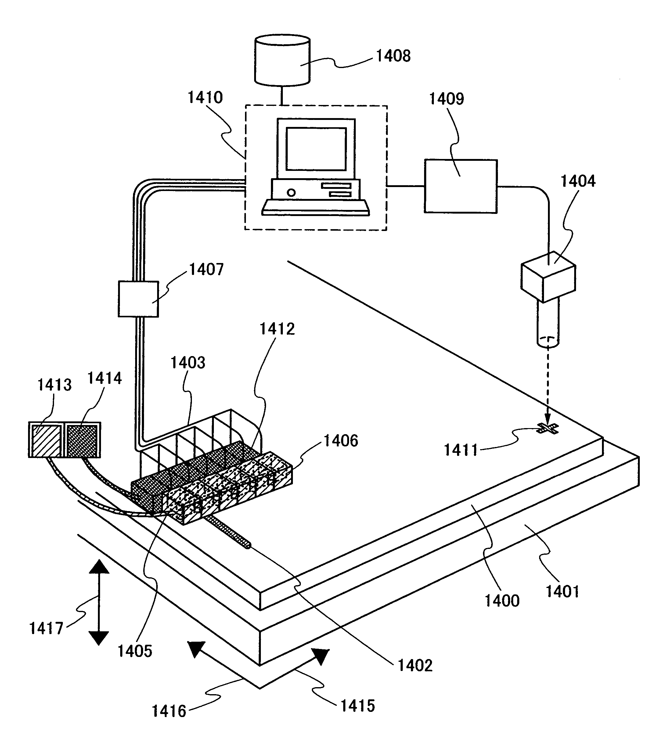
[0017]One ink jet apparatus may be provided with a plurality of heads. By providing a plurality of heads, a larger area can be processed and the time required for the entire steps can be shortened.
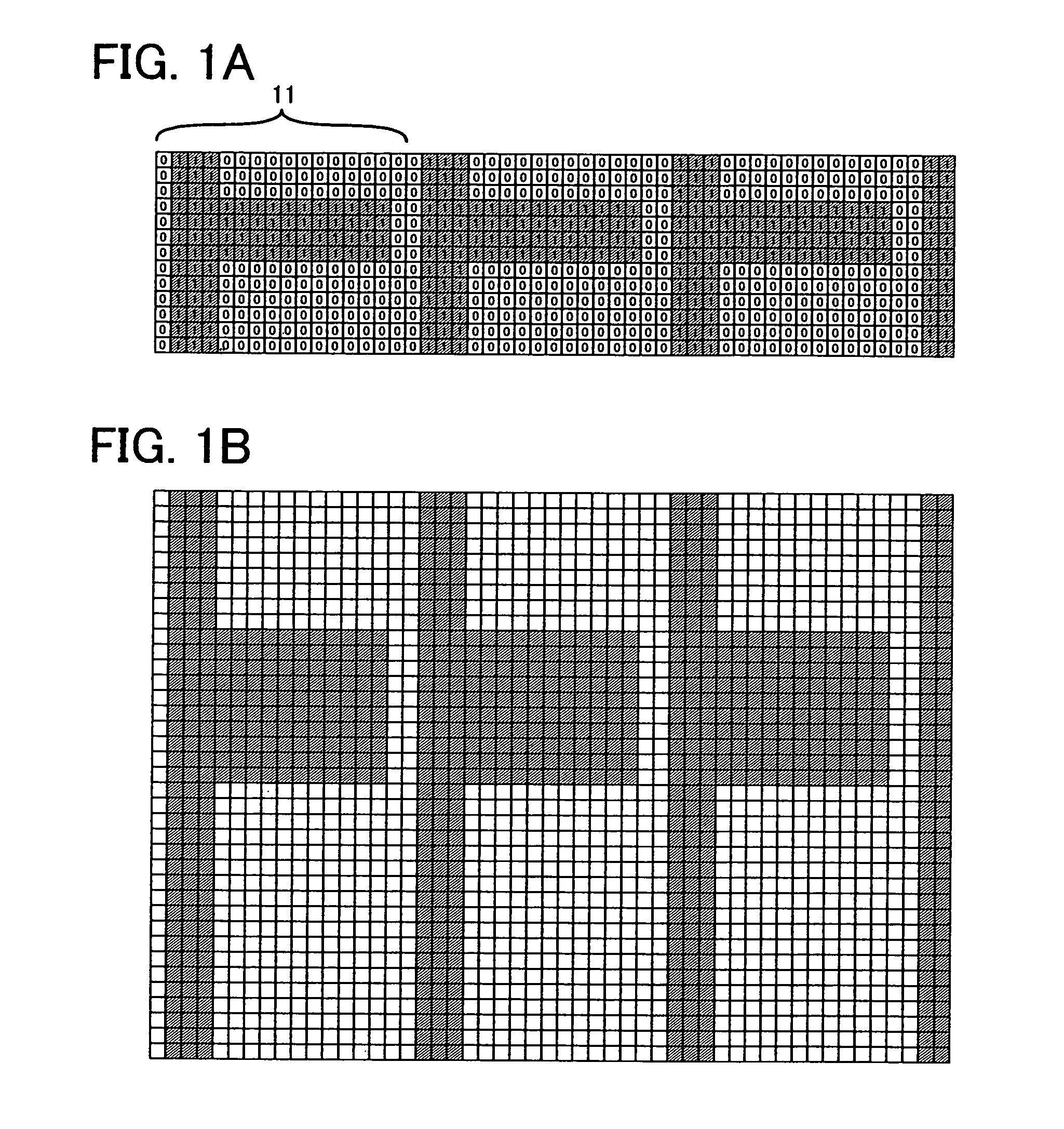
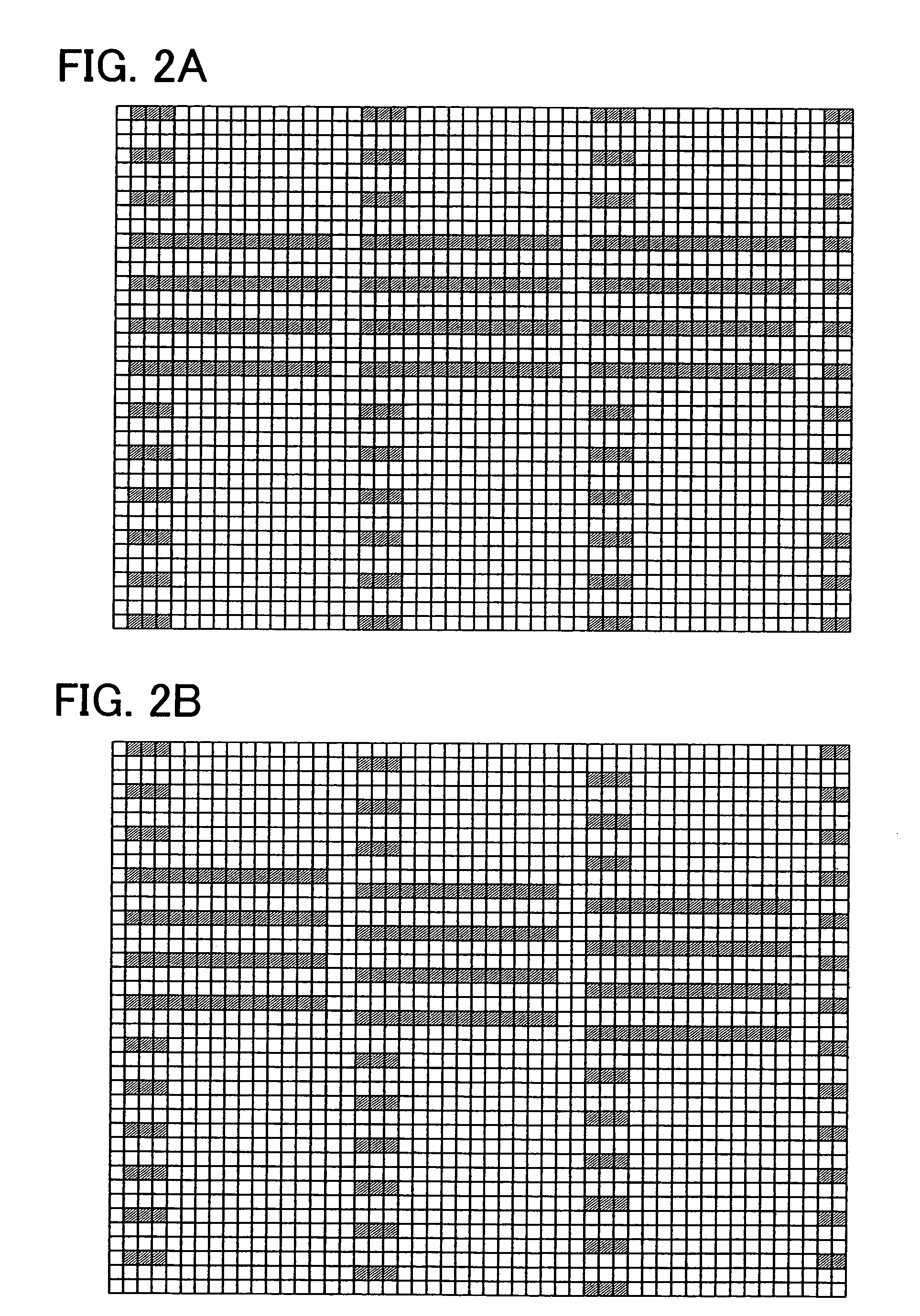
[0024]Therefore, according to one aspect of the present invention, after design diagram data of an electric circuit is created using a CAD tool, the design diagram data is converted into first raster data, which is then converted into second raster data. The first raster data is a square grid regarding a dot pitch Xdp in a horizontal direction and a dot pitch Ydp in the perpendicular direction as one unit. The second raster data is a rectangular grid regarding the dot pitch Xdp in the horizontal direction and a dot pitch Ydp / V (V>1) as one unit. The value of V, which is an indicator of segmentation, can be appropriately determined by a designer. By increasing V, the raster data can be further segmented. When discharging is conducted based on thus segmented raster data, discharging control with higher accuracy can be achieved.
[0035]In this specification, the main scanning direction indicates a direction where an object to be processed such as a substrate is to be delivered, and a direction perpendicular to the main scanning direction is called the sub scanning direction. A head having nozzles in a row has limitation on the arrangement density of nozzles in production of the head. Thus, when the major axis of the head is tilted to the sub scanning direction to conduct scanning in the main scanning direction, each nozzle can be used efficiently to shorten the process time.
[0036]In addition, the process time may be shortened by arranging nozzles in two or more rows. Furthermore, the process time may be shortened by providing a plurality of heads in one ink jet apparatus.
[0042]According to the present invention, discharging control with higher accuracy can be achieved by correcting with the use of segmented raster data.

Problems solved by technology

It is difficult to understand a circuit structure and a wire position just by this raster data.
Moreover, circuit design is also difficult just by raster data from the beginning.

Method used


Image

  • Method for manufacturing semiconductor device
  • Method for manufacturing semiconductor device
  • Method for manufacturing semiconductor device

Examples


embodiment mode 1

[0068]A flow chart from designing to droplet discharging is shown in FIG. 4. In order to manufacture a desired semiconductor device, first, each part is designed by a computer with a CAD tool (S401). A design diagram is created for each layer (a design diagram for a light-exposure mask, a doping mask, or the like).

[0069]After completing the designs, a design diagram of a material layer to be formed by an ink jet apparatus is selected and taken out from among those design diagrams (S402). The entire semiconductor device may be formed by an ink jet apparatus if possible.

[0070]The ink jet apparatus is provided with a head having an A number of nozzles (A is an integer of 2 or more) in a row, and droplets are discharged from different nozzles by changing a relative position between the head and an object to be processed, here a substrate. In order to discharge a droplet of a material through a binarizing process or a value-multiplexing process, the ink jet apparatus converts the design ...

embodiment mode 2

[0078]Here, description is made of an example for forming a wire in the following manner: a metal film is formed over a substrate having an insulating surface by a sputtering method, a resist material is discharged by an ink jet apparatus, and the metal film is etched by using the obtained resist material layer as a mask.

[0079]First, a tungsten film is formed over a glass substrate (5 inch on a side) by a sputtering method. Then, a resist material layer is dripped over the tungsten film by an ink jet apparatus (with a nozzle pitch of 507.5 μm and an upper limitation on discharging position accuracy of 6 μm), and then the resist material layer is baked. Prior to the dripping by the ink jet apparatus, the surface of the tungsten film may be coated with a silane coupling agent represented by a chemical formula Rn—Si—X(4-n) (n=1, 2, 3). By using a fluorine-based silane coupling agent (fluoroalkylsilane (FAS)) having a fluoroalkyl group in R as a typical example of a silane coupling agen...

embodiment mode 3

[0091]In accordance with the present invention, a semiconductor device or a display device is manufactured in such a way that at least one of constituents required for forming the semiconductor device, the display device, or the like, such as a conductive layer for forming a wiring layer or an electrode or a mask layer for forming a desired pattern is formed by a method capable of selectively forming in a desired shape. In the present invention, the constituents (also called patterns) are a conductive layer such as a wiring layer, a gate electrode layer, a source electrode layer, or a drain electrode layer, a semiconductor layer, a mask layer, an insulating layer, and the like and include all the constituents formed to have a predetermined shape. As the method capable of selectively forming an object in a desired pattern, a droplet discharging setting) method (also called an ink jet method depending on its system) capable of forming a conductive layer, an insulating layer, or the li...


PUM


Abstract

In the case of forming fine wires and the like by a droplet discharging apparatus to manufacture electric circuits, discharging controls including controls of a discharging position, a discharging timing, and the like are required to have very high accuracy. After forming design diagram data of an electric circuit by a CAD tool, the design diagram data is converted into first raster data, which is then converted into second raster data. The first raster data is a square grid regarding a dot pitch Xdp in a horizontal direction and a dot pitch Ydp in a perpendicular direction as one unit. The second raster data is a rectangular grid regarding the dot pitch Xdp in the horizontal direction and a dot pitch Ydp / V (V>1) as one unit. It is to be noted that arbitrary discharging number is the same before and after the conversion from the first raster data to the second raster data.

Description

BACKGROUND OF THE INVENTION[0001]1. Field of the Invention[0002]The present invention relates to a semiconductor device having a circuit which includes a thin film transistor (hereinafter called a TFT), and a manufacturing method thereof. For example, the present invention relates to an electronic appliance in which an electro-optic device typified by a liquid crystal display panel or a light-emitting display device having an organic light-emitting element is mounted as a part thereof.[0003]In this specification, the semiconductor device includes general semiconductor devices that can function by using semiconductor characteristics, and an electro-optical device, a semiconductor circuit, and an electronic appliance are all included in the semiconductor device.[0004]2. Description of the Related Art[0005]In recent years, attention has been focused on a technique for forming a thin film transistor (TFT) using a semiconductor thin film (with a thickness of about several nanometers to s...

Claims


Application Information

Patent Timeline
Patent Type & Authority Patents(United States)
IPC IPC(8): G06F19/00
CPCH01L27/12H01L27/1292H01L27/1285H01L51/0022H10K71/611H01L27/1214
Inventor FUJII, GENSATO, EIJIONOYA, SHIGERU
Owner SEMICON ENERGY LAB CO LTD
Learn More