Dual top gas feed through distributor for high density plasma chamber

a plasma chamber and distributor technology, applied in the direction of chemical vapor deposition coating, coating, electric discharge tube, etc., can solve the problems of difficult to completely fill the high-aspect-ratio gap using conventional cvd techniques, the number of persistent challenges in achieving the desired deposition properties, and the relative poor gapfill ability, etc., to achieve the effect of improving the uniformity of the sio2 layer and improving the uniformity of the layer

Inactive Publication Date: 2010-07-20
APPLIED MATERIALS INC
View PDF67 Cites 308 Cited by
  • Summary
  • Abstract
  • Description
  • Claims
  • Application Information

AI Technical Summary

Benefits of technology

[0017]Embodiments of the present invention provide improved uniformity in a layer of material deposited on a semiconductor substrate, for example improved uniformity of an SiO2 layer. In particular, embodiments of the present provide channels to inject a fluid, for example O2 gas, centrally from a gas distributor to avoid deposition of a silicon rich layer centrally on the wafer.

Problems solved by technology

One persistent challenge faced by semiconductor manufacturers in the design and fabrication of such densely packed integrated circuits is the desire to prevent spurious interactions between circuit elements, a goal that has required ongoing innovation as geometry scales continue to decrease.
High-aspect-ratio gaps are difficult to fill completely using conventional CVD techniques, which tend to have relatively poor gapfill abilities.
Even with the use of HDP and ICP processes, there remain a number of persistent challenges in achieving desired deposition properties.
These include the need to manage thermal characteristics of the plasma within a processing chamber, particularly with high-energy processes that may result in temperatures that damage structures in the chamber.
Nonuniformities lead to inconsistencies in device performance and may result from a number of different factors.
One particular challenge with HDP and ICP processes is the management of chemical reactions during the deposition process so that the chemical characteristics of the layer deposited with the HDP / CVD process are uniform across the area wafer.

Method used


Image

  • Dual top gas feed through distributor for high density plasma chamber
  • Dual top gas feed through distributor for high density plasma chamber
  • Dual top gas feed through distributor for high density plasma chamber

Examples


Embodiment Construction

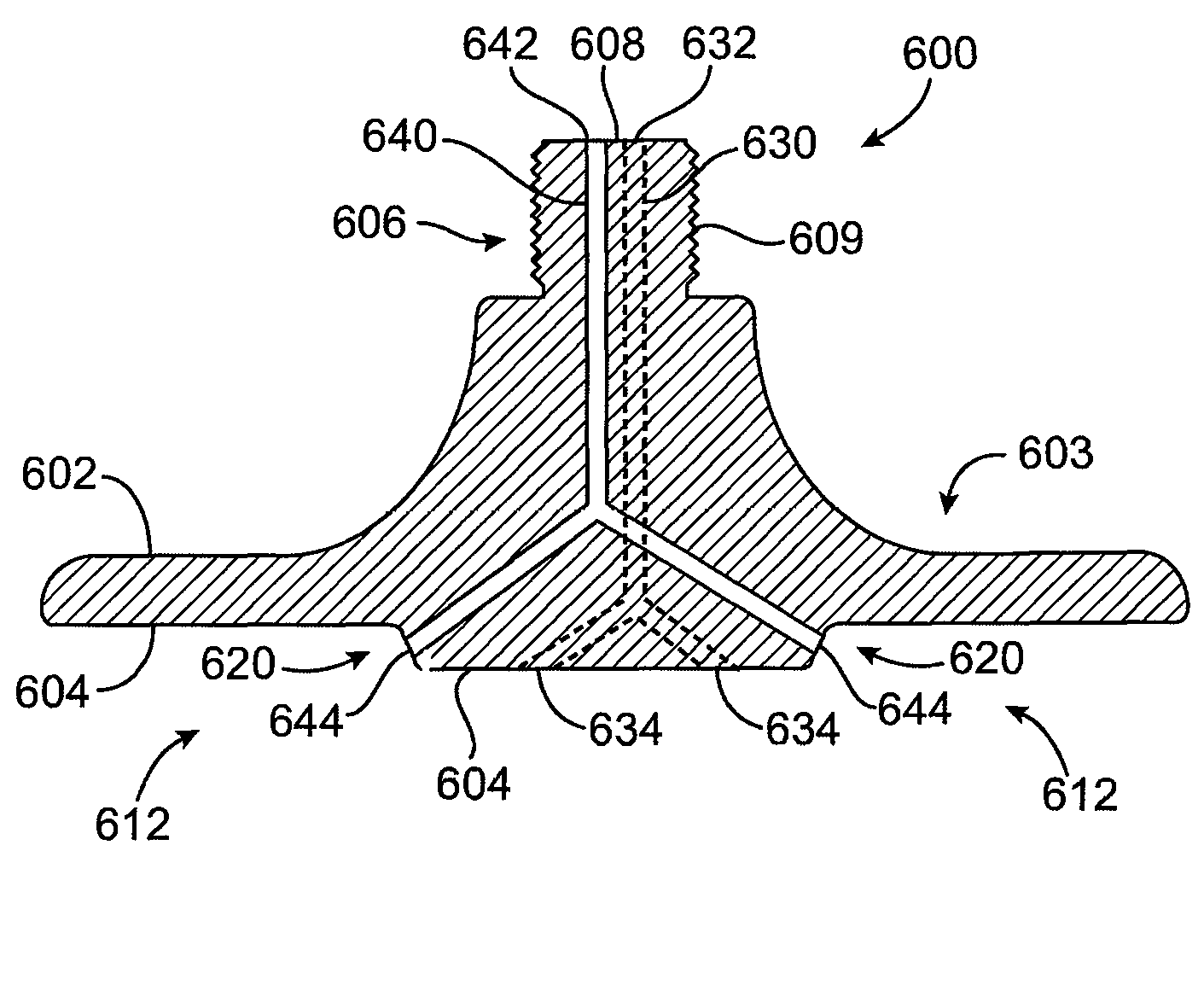
[0032]According to the present invention, methods and apparatus related to the field of semiconductor processing equipment are provided. More particularly, the present invention relates to methods and apparatus for depositing thin films, for example with gas distributors, used in the formation of integrated circuits. Merely by way of example, the method and apparatus of the present invention are used in HDP / CVD processes. The method and apparatus can be applied to other processes for semiconductor substrates, for example those used in the formation of integrated circuits.

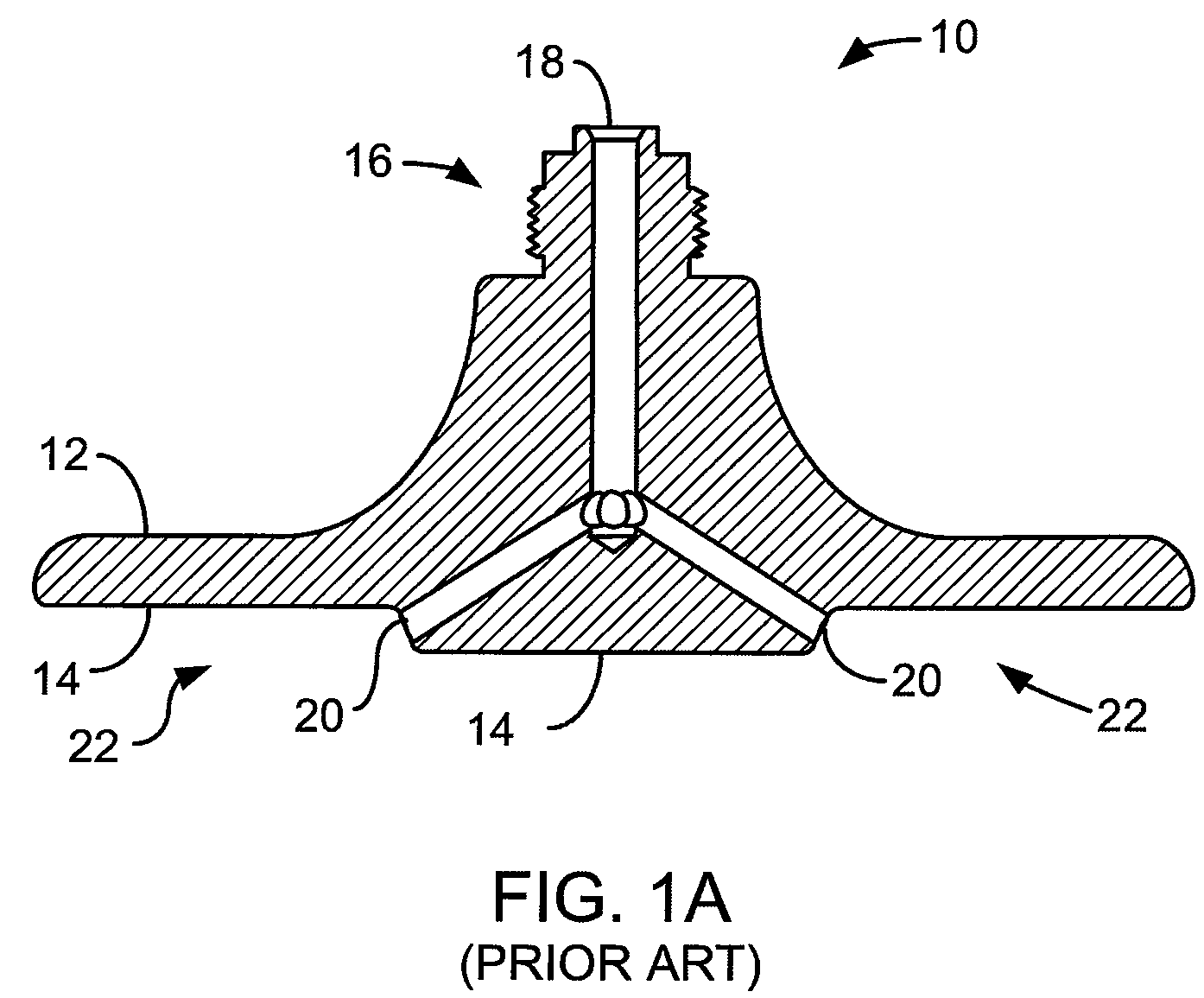
[0033]FIG. 1A shows a previously known gas distributor. Gas distributor 10 has a gas deflecting surface 12 and a gas distributor face 14. Gas deflecting surface 12 provides a pathway for cleaning gases during a chamber clean process. Cleaning gases are directed to the chamber walls instead of a substrate support member located directly below the gas distributor. The gas distributor 10 is connected to a chamber wall ...


PUM

PropertyMeasurementUnit
temperatureaaaaaaaaaa
pressuresaaaaaaaaaa

Abstract

A gas distributor for use in a semiconductor process chamber comprises a body. The body includes a first channel formed within the body and adapted to pass a first fluid from a first fluid supply line through the first channel to a first opening. A second channel is formed within the body and adapted to pass a second fluid from a second fluid supply line through the second channel to a second opening. The first and second openings are arranged to mix the fluids outside the body after the fluids pass through the openings.

Description

BACKGROUND OF THE INVENTION[0001]The present invention relates generally to the field of semiconductor processing equipment. More particularly, the present invention relates to methods and apparatus for depositing thin films, for example with gas distributors, used in the formation of integrated circuits.[0002]One of the primary steps in the fabrication of modem semiconductor devices is the formation of a film, such as a silicon oxide film, on a semiconductor substrate. Silicon oxide is widely used as dielectric layer in the manufacture of semiconductor devices. As is well known, a silicon oxide film can be deposited by a thermal chemical-vapor deposition (“CVD”) process or by a plasma-enhanced chemical-vapor deposition (“PECVD”) process. In a conventional thermal CVD process, reactive gases are supplied to a surface of the substrate, where heat-induced chemical reactions take place to produce a desired film. In a conventional plasma-deposition process, a controlled plasma is formed...

Claims


Application Information

Patent Timeline
Patent Type & Authority Patents(United States)
IPC IPC(8): C23C16/455H01L21/306C23F1/00C23C16/06C23C16/22
CPCC23C16/4405C23C16/45574C23C16/45591H01J37/3244H01J37/32449
Inventor BANG, WON B.NEMANI, SRIVIVAS D.PHAM, PHONGYIEH, ELLIE Y.
Owner APPLIED MATERIALS INC
Why Eureka
Try Eureka