Material and method of manufacture of a solder joint with high thermal conductivity and high electrical conductivity

a solder joint and high electrical conductivity technology, applied in the field of materials technology, can solve the problems of material melting point well beyond the manufacturing temperature, the design limit of the package becomes the interface between the ic and the package, and the design limit of the package becomes the limit of the package, so as to improve increase thermal and electrical conductivity, and high conductivity

Active Publication Date: 2010-07-20
SULZER METCO (US) INC
View PDF3 Cites 10 Cited by
  • Summary
  • Abstract
  • Description
  • Claims
  • Application Information

AI Technical Summary

Benefits of technology

[0010]By combining a solder material and high conductivity (thermal and electrical) material, it is possible to create a composite material that is both solderable at a low temperature and has increased thermal and electrical conductivity compared to using solder alone. The present invention provides a powder blend or composite powder that is fed into a kinetic spray device, accelerated towards a substrate or part in order to form a composite solder with thermal and electrical properties better than conventional solders. The other advantages of building a solder layer in this manner include a low oxide content to improve subsequent solderability, excellent control of the deposition thickness, excellent control of the deposition chemistry and lastly, high speed of manufacture.

Problems solved by technology
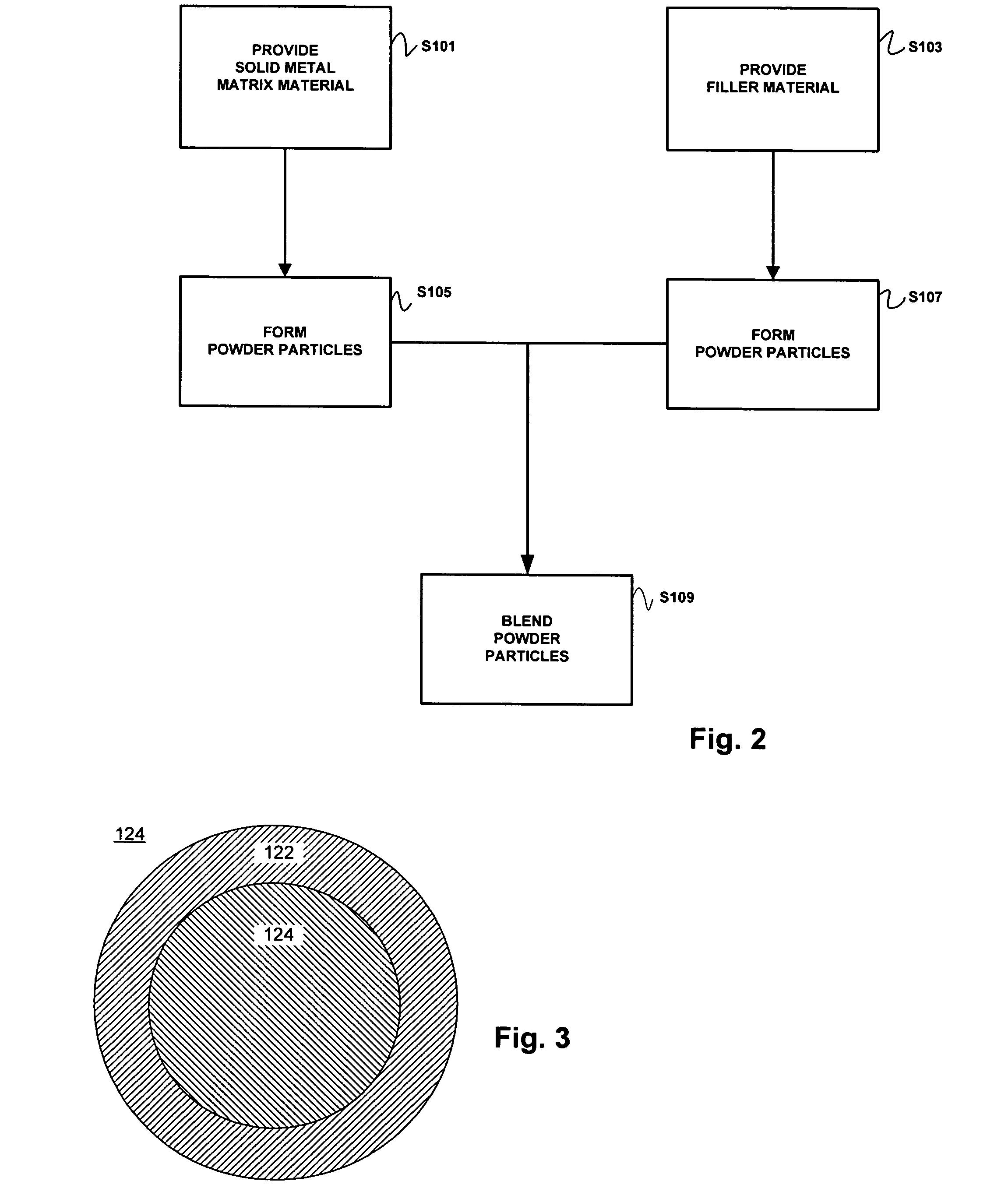
The packaging method for an IC becomes a limiting factor, as the package serves the function of carrying high current densities in addition to high thermal loads.
In some cases, the design limit of the package becomes the interfaces between the IC and the package, which is itself limited by the manufacturing technique used.
However, these material also have melting points well beyond the manufacturing temperatures that can be tolerated for the IC.
But these solders do not have an ability to move heat and electrons as well as the interface materials themselves and thus limit the performance potential of the package.
The thickness of the solder layer is limited by the tolerance of the IC and package in addition to the manufacturing method used.

Method used


Image

  • Material and method of manufacture of a solder joint with high thermal conductivity and high electrical conductivity
  • Material and method of manufacture of a solder joint with high thermal conductivity and high electrical conductivity
  • Material and method of manufacture of a solder joint with high thermal conductivity and high electrical conductivity

Examples


Embodiment Construction

[0024]Reference will now be made in detail to the preferred embodiments of the present invention, examples of which are illustrated in the accompanying drawings.

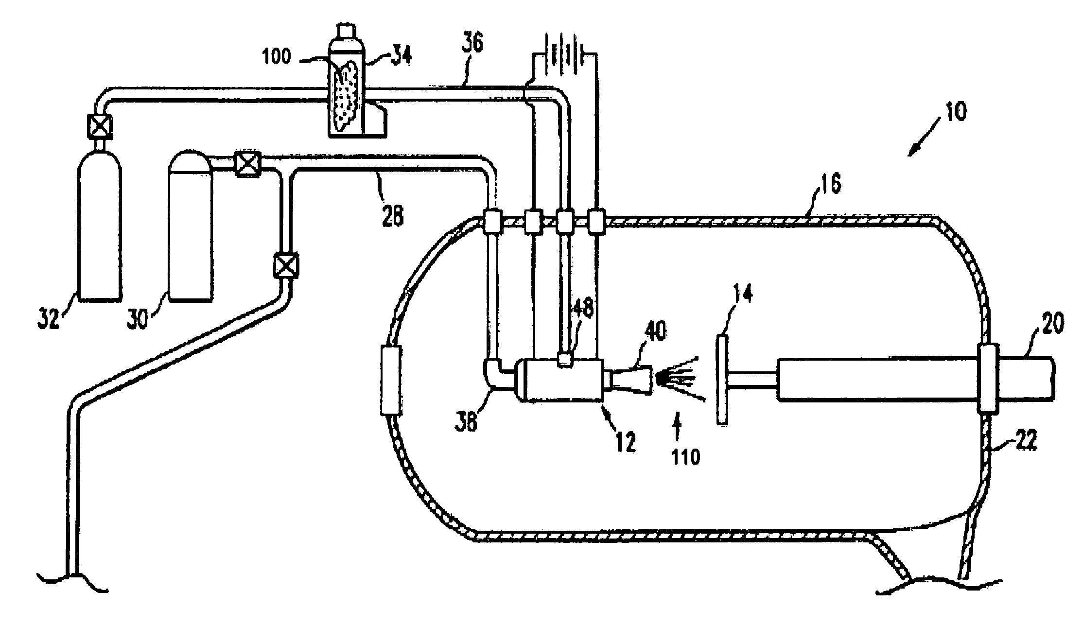
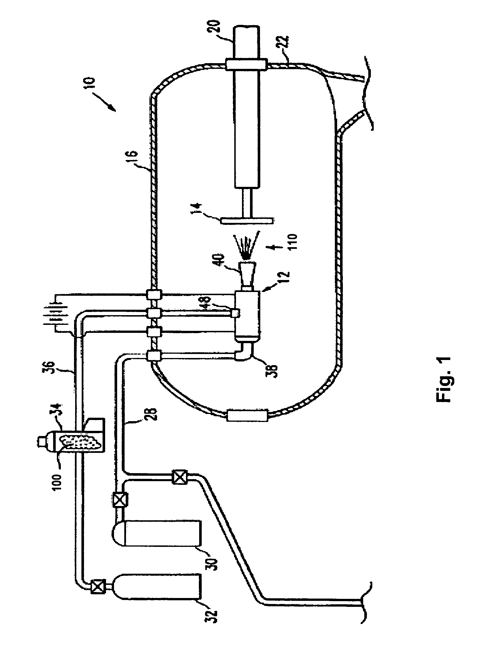
[0025]The composite material of the present invention may be used in a kinetic spray system. FIG. 1 shows a kinetic spray system 10 for use in accordance with the present invention. The system 10 includes a kinetic spray gun 12 which is mounted together with a workpiece 14 within the hollow interior of a vacuum tank 16. The kinetic spray gun 12 is disposed relative to the workpiece 14 for directing a spray 110 onto the workpiece 14. The workpiece 14 may be mounted on a workpiece manipulation device 20 mounted through a wall of the vacuum tank 16 and extending into the interior of the vacuum tank 16.

[0026]As shown in the typical system 10 of FIG. 1, the kinetic spray gun 12 produces a cold spray for direction onto the workpiece 14 in response to a main gas flow under pressure and a powder gas which carries a composite powder ...


PUM

PropertyMeasurementUnit
volume fractionaaaaaaaaaa

Abstract

The present invention provides a powder blend or composite powder that is fed into a kinetic spray device, accelerated towards a substrate or part in order to form a composite solder with thermal and electrical properties better than existing solder. The other advantages of building a solder layer in this manner include a low oxide content to improve subsequent solderability, excellent control of the deposition thickness, excellent control of the deposition chemistry and lastly, high speed of manufacture.

Description

CROSS REFERENCE TO RELATED APPLICATIONS[0001]Not ApplicableSTATEMENT REGARDING FEDERALLY SPONSORED RESEARCH OR DEVELOPMENT[0002]Not ApplicableREFERENCE TO A “MICROFICHE APPENDIX”[0003]Not ApplicableBACKGROUND OF THE INVENTION[0004]1. Field of the Invention[0005]The present invention relates generally to the field of materials technology and more particularly to a solder composition having improved thermal and electrical properties and a method for manufacturing the same.[0006]2. Description of the Related Art[0007]In any circuit involving electrical power, a major design objective is to reduce the temperature of the components, improve reliability, reduce cost, and improve operation. Many integrated circuits (“ICs”)—including, for example, dual in-line plastic packaged ICs—have shapes not conducive to fastening directly to the chassis. The packaging method for an IC becomes a limiting factor, as the package serves the function of carrying high current densities in addition to high t...

Claims


Application Information

Patent Timeline
Patent Type & Authority Patents(United States)
IPC IPC(8): B05D1/12B22F1/17
CPCB22F1/025B23K35/0244B23K35/025B23K35/26B23K35/262B23K35/30B23K35/3006B23K35/3013B23K35/302B23K35/3033B23K35/36B23K35/383C23C4/12C23C24/04H05K3/3484B22F3/115Y10T428/12181H05K2201/0215H05K2201/0218H05K2203/0425H05K2203/1344H05K3/3485B22F1/17
Inventor SCHMID, RICHARD K.DOESBURG, JACOBUS C.
Owner SULZER METCO (US) INC
Why Eureka
Try Eureka