
Method for manufacturing semiconductor optical device

a manufacturing method and optical device technology, applied in semiconductor lasers, semiconductor devices, electrical devices, etc., can solve the problems of increasing the operating resistance, reducing the device resistance, and reducing the impurity density of the bdr layer, so as to prevent the operating resistance of the device from deviating, and the impurity diffusion is reduced.

Inactive Publication Date: 2010-07-20
MITSUBISHI ELECTRIC CORP
View PDF14 Cites 1 Cited by
  • Summary
  • Abstract
  • Description
  • Claims
  • Application Information

AI Technical Summary

Benefits of technology

[0006]The present invention has been devised to solve the above problem. It is, therefore, an object of the present invention to provide a method for manufacturing a semiconductor optical device in such a way as to reduce the impurity diffusion from the BDR layer to the contact layer to prevent the operating resistance of the device from deviating from the design value.

Problems solved by technology

First, this semiconductor laser includes a BDR (Band Discontinuity Reduction) layer disposed between a contact layer and a cladding layer to reduce the band discontinuity between these contact and cladding layers and thereby reduce the device resistance.
This thermal diffusion leads to a reduction in the impurity density of the BDR layer and hence an increase in the operating resistance of the semiconductor optical device, with the result that the operating resistance of the device deviates from the design value.

Method used


Image

  • Method for manufacturing semiconductor optical device
  • Method for manufacturing semiconductor optical device
  • Method for manufacturing semiconductor optical device

Examples


first embodiment

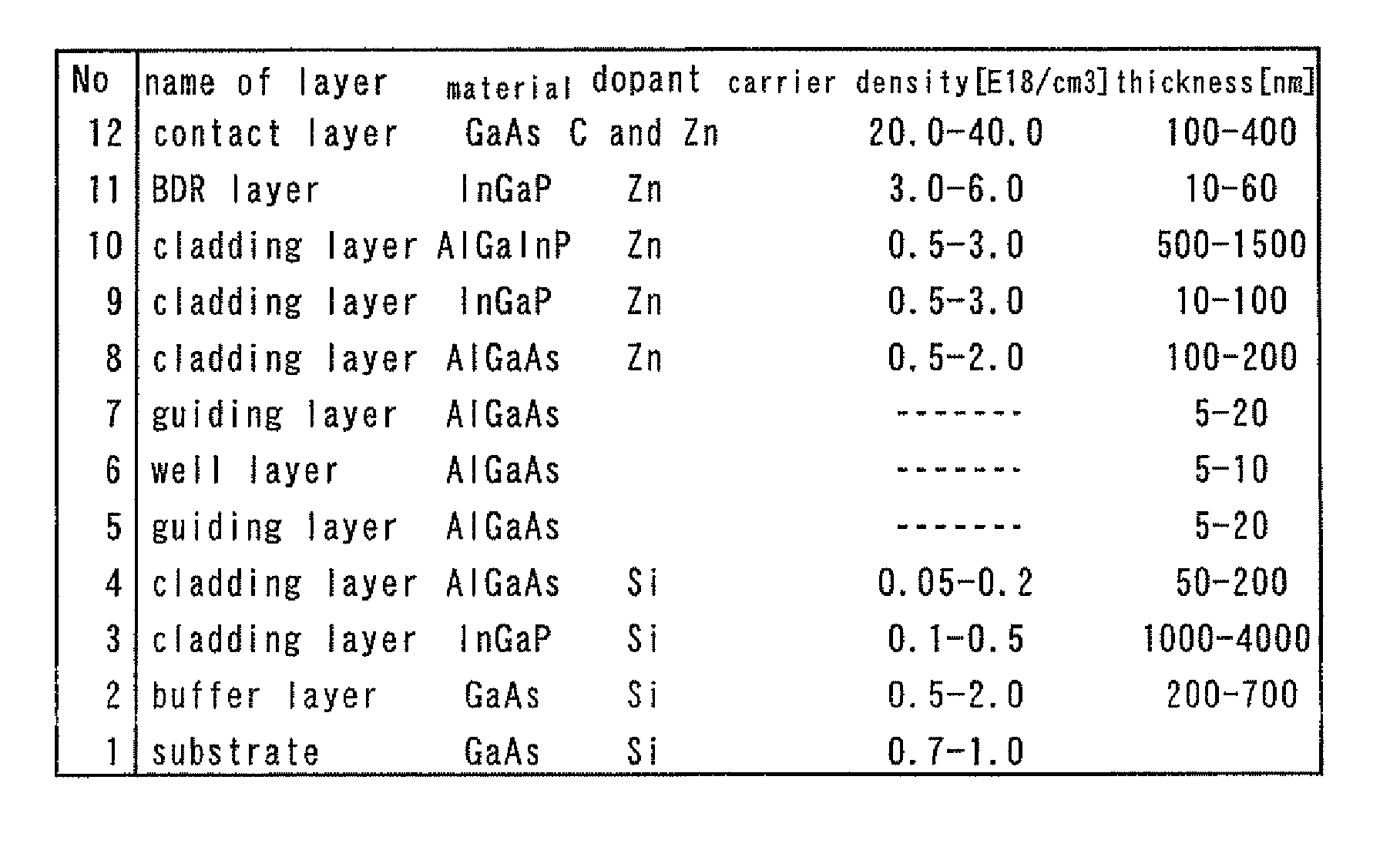
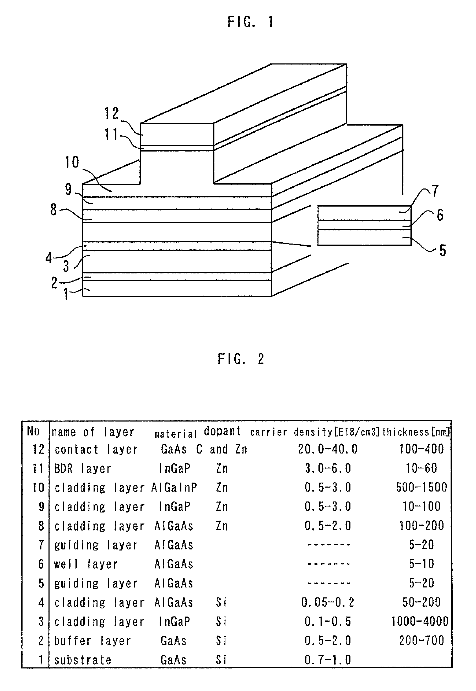
[0018]FIG. 1 is a diagram illustrating the configuration of a semiconductor laser according to a first embodiment of the present invention. It should be noted that in FIGS. 1 and 2, the same reference numerals are used to designate the same layers. FIG. 2 shows the name, material, dopant, carrier concentration, and thickness of each layer in the semiconductor laser. These layers will now be described.

[0019]First, a buffer layer 2 of Si—GaAs, i.e., GaAs doped with Si (an n-type dopant), is formed on a GaAs substrate 1. Then, a cladding layer 3 of Si—InGaP (or Si-doped InGaP) is formed on the buffer layer 2, and a cladding layer 4 of Si—AlGaAs (or Si-doped AlGaAs) is formed on the cladding layer 3. The buffer layer is provided to enhance the crystallinity of the device on the substrate. Further, the primary functions of the cladding layers are to increase the carrier densities of the guiding layer and the quantum well layer (formed later) thereon and to confine light within the active...


PUM


Abstract

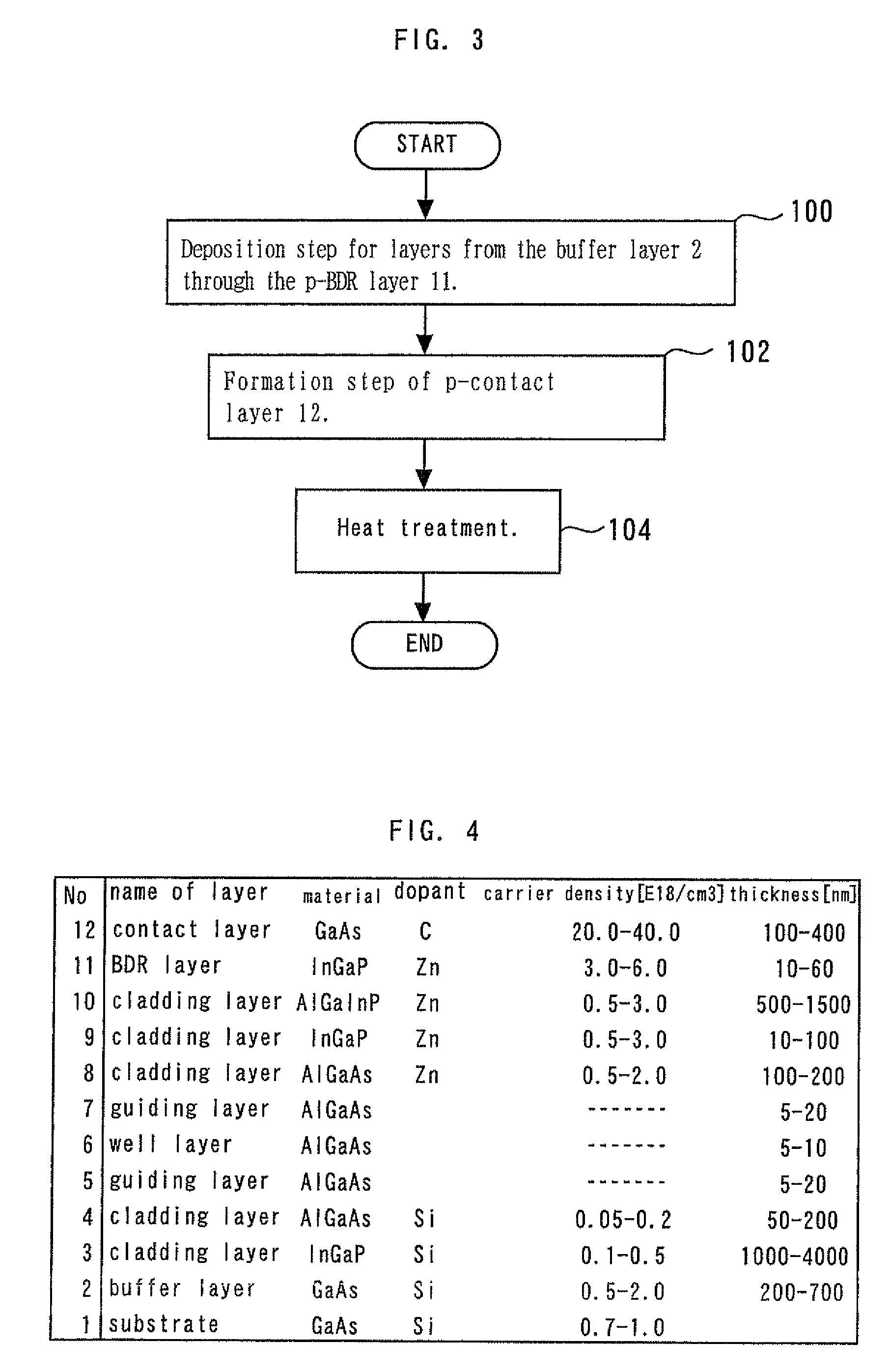
A method for manufacturing a semiconductor optical device includes forming a BDR (Band Discontinuity Reduction) layer of a first conductivity type doped with an impurity, depositing a contact layer of the first conductivity type in contact with the BDR layer after forming the the BDR layer, the contact layer being doped with the same impurity as the BDR layer and used to form an electrode, and heat treating after forming the contact layer.

Description

BACKGROUND OF THE INVENTION[0001]1. Field of the Invention[0002]The present invention relates to a method for manufacturing a semiconductor optical device, and more particularly to a method for manufacturing a semiconductor optical device in such a way that the operating resistance of the device does not deviate from the design value.[0003]2. Background Art[0004]Semiconductor lasers have been widely used in optical disc drives, scanners, copiers, etc. JP-A-11-307810 (1999) discloses such a semiconductor laser, which has two important features. First, this semiconductor laser includes a BDR (Band Discontinuity Reduction) layer disposed between a contact layer and a cladding layer to reduce the band discontinuity between these contact and cladding layers and thereby reduce the device resistance. This BDR layer has an energy bandgap intermediate between the energy bandgaps of the contact layer and the cladding layer. Second, the contact layer is doped with C to reduce the contact resis...

Claims


Application Information

Patent Timeline
Patent Type & Authority Patents(United States)
IPC IPC(8): H01L21/00H01L33/26H01L33/36
CPCH01S5/0421H01L33/02H01L33/305H01S5/3054
Inventor HANAMAKI, YOSHIHIKOONO, KENICHI
Owner MITSUBISHI ELECTRIC CORP
Learn More