
Method of adjusting a threshold voltage of a multi-gate structure device

Inactive Publication Date: 2015-07-23
PEKING UNIV
View PDF1 Cites 0 Cited by
  • Summary
  • Abstract
  • Description
  • Claims
  • Application Information

AI Technical Summary

Benefits of technology

This patent describes a solution to reduce the impact of impurities on electronic devices, in order to maintain higher levels of mobility and performance. The solution involves depositing a passivation layer to prevent loss of doped impurities during annealing, followed by advanced annealing techniques to form a shallow junction. This approach allows for a larger range of threshold voltage options, while minimizing the negative effects of impurity scattering on carrier mobility. The method is compatible with conventional CMOS processes and can be applied to large-scale production.

Problems solved by technology

After entering the 22 nm technology node, in a conventional planar field effect transistor a leakage current is increasing due to a growing short channel effect, which can not meet the development of semiconductor manufacturing.
Although the multi-gate structure device itself has a characteristic geometry structure, so that it has excellent gate control performance, this will make a body effect factor decrease.
Accordingly, in comparison to a conventional planar device, it is difficult to achieve a multi-threshold device from a multi-gate structure device.
However, due to the presence of Coulomb impurity scattering, improvement of a channel doping concentration will seriously affect the mobility of carriers in the device, finally so that the driving current is dropped significantly.
This is one of the major difficulties and challenges when a multi-gate structure device is applied to a large scale integrated circuit product.

Method used


Image

  • Method of adjusting a threshold voltage of a multi-gate structure device
  • Method of adjusting a threshold voltage of a multi-gate structure device
  • Method of adjusting a threshold voltage of a multi-gate structure device

Examples


Embodiment Construction

[0025]Hereinafter, the present invention will be described in detail in conjunction with the specific embodiments. Specifically, this is to provide a process solution that achieves a multi-threshold voltage of a multi-gate structure device proposed by the present invention, and a three-gate structure device is taken for example (Obviously, the solutions of the present invention is fully applicable to the other multi-gate structures), but it is not to limit the scope of the present invention in any ways.

[0026]A n-type three-gate field effect transistor with a Fin strip having a width of about 10 nm, a height of 30 nm and a channel length of about 25 nm is prepared according to the following steps:

[0027]1) highly doping the channel surface, with a doping dose of 1e15 cm−2, by a plasma impurity doping technology, a silicon epitaxial in situ doping technology or a monolayer doping technology;

[0028]2) depositing oxide silicon to a thickness of 100 Å by Atomic Layer Deposition;

[0029]3) ac...


PUM


Abstract

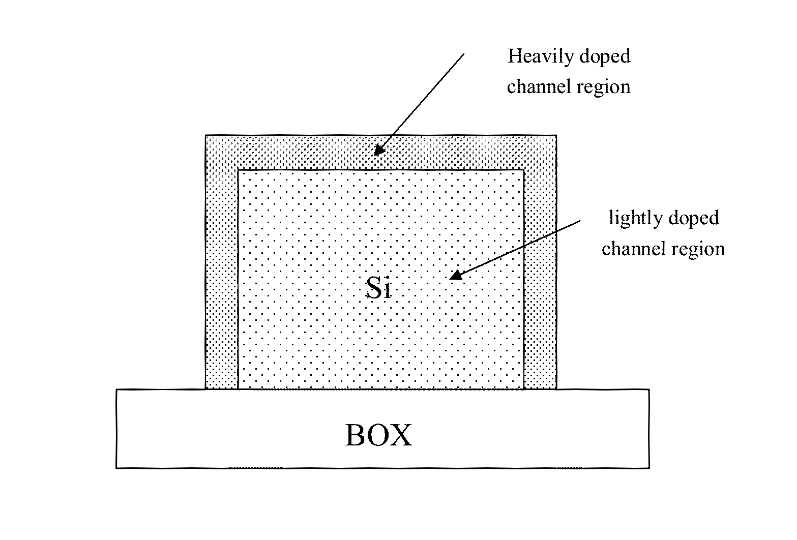
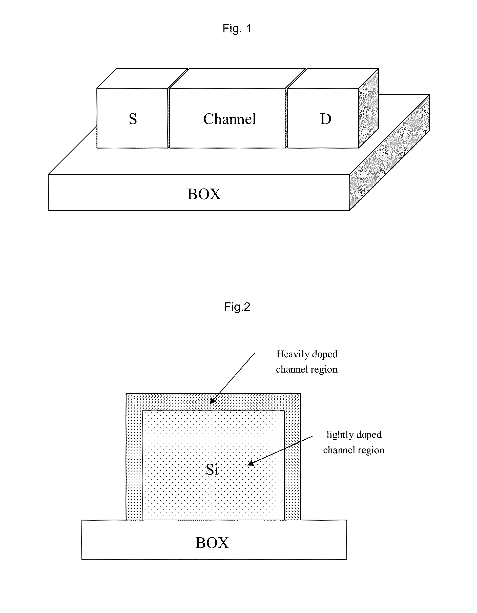
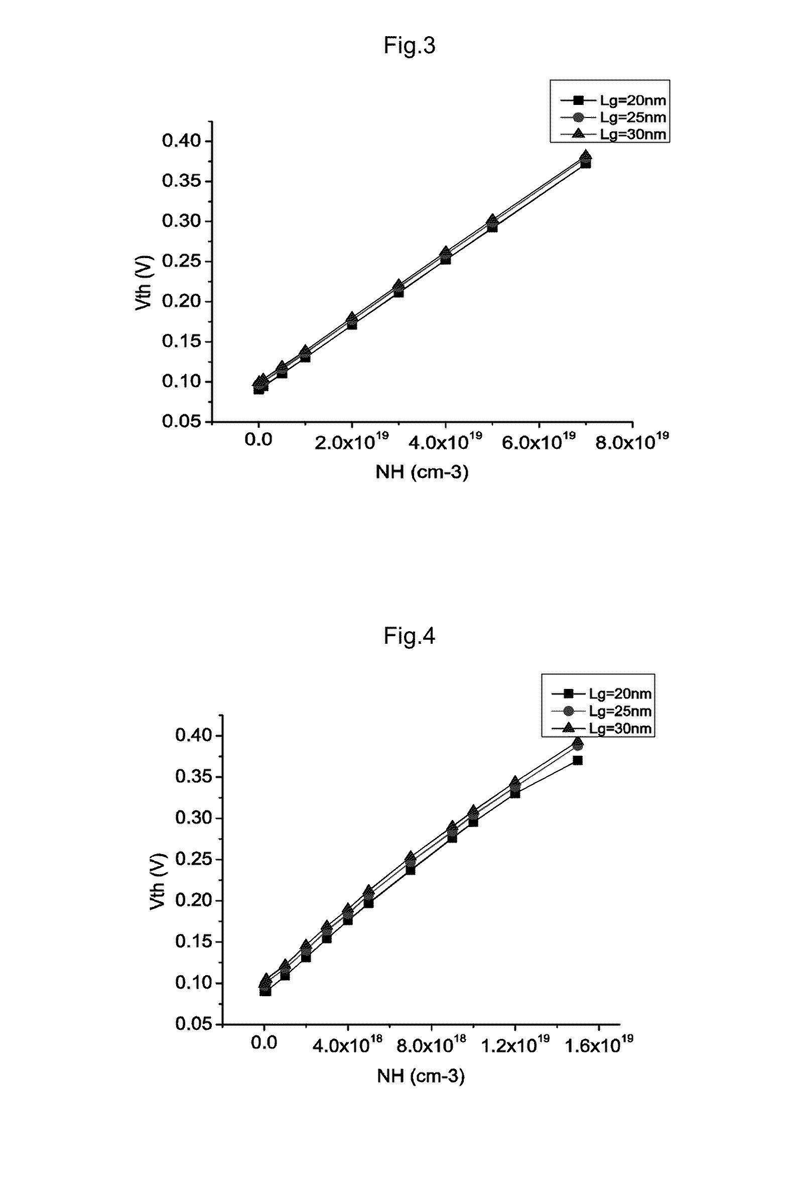
The present invention discloses a method of adjusting a threshold voltage of a multi-gate structure device, wherein, preparing the multi-gate structure device to be formed to have a channel impurity distribution with high doping on surface and lowly doping inside, where while a threshold voltage is adjusted by using impurity doping, the influences of the Coulomb impurity scattering on the carriers is reduced as much as possible, so that the mobility of the carriers is maintained at a higher level. Firstly, the present solution is able to make a multi-gate device obtain a larger range of a multi-threshold voltage; it is convenient for the various demands of the device in the circuit designing by IC designers. Secondly, in the course of introducing the impurity doping to adjust a threshold voltage, the influences of the Coulomb impurity scattering on the channel carrier are reduced as much as possible, so that the mobility of the charge carriers is maintained at a higher level, and the device is ensured to have a higher drive current. Finally, the present solution is achieved by the process method compatible with a conventional CMOS, and has the potential for a large scale production.

Description

CROSS REFERENCE OF RELATED APPLICATIONS[0001]This application is a 371 U.S. Nationalization of Patent Cooperation Treaty Application PCT / CN2013 / 084739, filed Sep. 30, 2013, which claims the benefit of Chinese Patent Application No. 201310103272.X, filed on Mar. 28, 2013, each of which are incorporated herein by reference in their entirety.TECHNICAL FIELD[0002]The present invention relates to a method of adjusting a threshold voltage of a multi-gate structure device, which belongs to a field of ultra large scale integrated circuit manufacturing technology.BACKGROUND OF THE INVENTION[0003]Today's semiconductor manufacturing industry is rapidly developing under the guidance of Moore's Law, so as to continuously improve performance and integration density of integrated circuits while reducing power consumption as much as possible. Preparation of a high-performance, low-power ultra short channel device becomes the focus of the future semiconductor manufacturing industry. After entering t...

Claims


Application Information

Patent Timeline
IPC IPC(8): H01L21/225H01L29/78H01L29/10
CPCH01L21/2252H01L29/7855H01L29/105H01L21/00H01L29/775H01L29/0673H01L29/66795H01L29/785
Inventor LI, MINGFAN, JIEWENLI, JIAXU, XIAOYANHUANG, RU
Owner PEKING UNIV
Learn More