Apparatus for effecting plasma chemical vapor deposition (PCVD)

a technology of apparatus and plasma, applied in the field of apparatus for effecting plasma chemical vapor deposition, can solve the problems of reducing the maximum microwave power supplied to the resonant cavity, significant signal attenuation, and deterioration of the rotational symmetry of the plasma, and achieves high microwave power levels and high deposition rates

Active Publication Date: 2010-07-20
DRAKA COMTEQ BV
View PDF13 Cites 8 Cited by
  • Summary
  • Abstract
  • Description
  • Claims
  • Application Information

AI Technical Summary

Benefits of technology

[0019]Accordingly, one aspect of the present invention is to provide an apparatus for carrying out a plasma chemical vapor deposition (PCVD) process in which the apparatus is capable of employing high microwave power levels to yield high deposition rates.
[0020]Another aspect of the present invention is to provide an apparatus for carrying out a plasma chemical vapor deposition (PCVD) process in which the transfer of energy from microwaves to the plasma in the waveguide is improved, if not optimized.
[0021]Yet another aspect of the present invention is to provide an apparatus for carrying out a plasma chemical vapor deposition (PCVD) process that reduces the undesirable reflection of microwaves during the passage of microwaves from a feed waveguide to a coaxial waveguide.
[0025]According to the present invention, the apparatus for carrying out a plasma chemical vapor deposition (PCVD) process typically employs an antenna that bisects the feed waveguide. When such a particular construction of the antenna in the coaxial waveguide is used, it is possible to omit the centering components from the coaxial waveguide. Because the antenna bisects the feed waveguide (and is partially located outside the microwave guide), centering of the antenna in the coaxial waveguide can be readily achieved.
[0026]Moreover, the configuration (i.e., construction) of the present PCVD apparatus simplifies cleaning of the resonant cavity if and when sparking occurs. This facilitates reuse of the resonant cavity, which, in turn, leads to considerable cost savings. Moreover, because the antenna bisects the feed waveguide and is partially located outside the feed waveguide, it is possible to cool the antenna using forced gas or liquid cooling. Such cooling may be necessary when high microwave power levels are employed. Furthermore, it has now been found that the configuration of the present PCVD apparatus makes maintaining the antenna at the central position in the coaxial waveguide less important to the proper operation of the PCVD apparatus.
[0027]In a particular embodiment of the present PCVD apparatus, a guide element is present in the interior of the feed waveguide at the point where the antenna bisects the feed waveguide. The guide element enables the microwaves to pass from the feed waveguide to the coaxial waveguide (i.e., facilitates passage of the microwaves into the coaxial waveguide). The guide element must be configured so that passage of microwaves from the feed portion to the coaxial portion of the waveguide will not cause reflection of microwaves, which adversely affects the microwave power supplied to the plasma zone. In this regard, the guide element typically embraces a conical or spherical shape.

Problems solved by technology

Over great lengths of the optical fiber, such defects may cause significant signal attenuation.
Unfortunately, increasing the resonant cavity's diameter to accommodate a thicker preform will cause the rotational symmetry of the plasma to deteriorate.
Moreover, such materials reduce the maximum microwave power supplied to the resonant cavity, which is attributable to their relatively low dielectric strength.
In addition, the present inventors have found that the surface roughness of such centering component materials introduces minor air channels, which adversely affect the performance of the resonant cavity.
Consequently, such centering components constitute an undesirable constraint for PCVD devices.

Method used


Image

  • Apparatus for effecting plasma chemical vapor deposition (PCVD)
  • Apparatus for effecting plasma chemical vapor deposition (PCVD)

Examples


Embodiment Construction

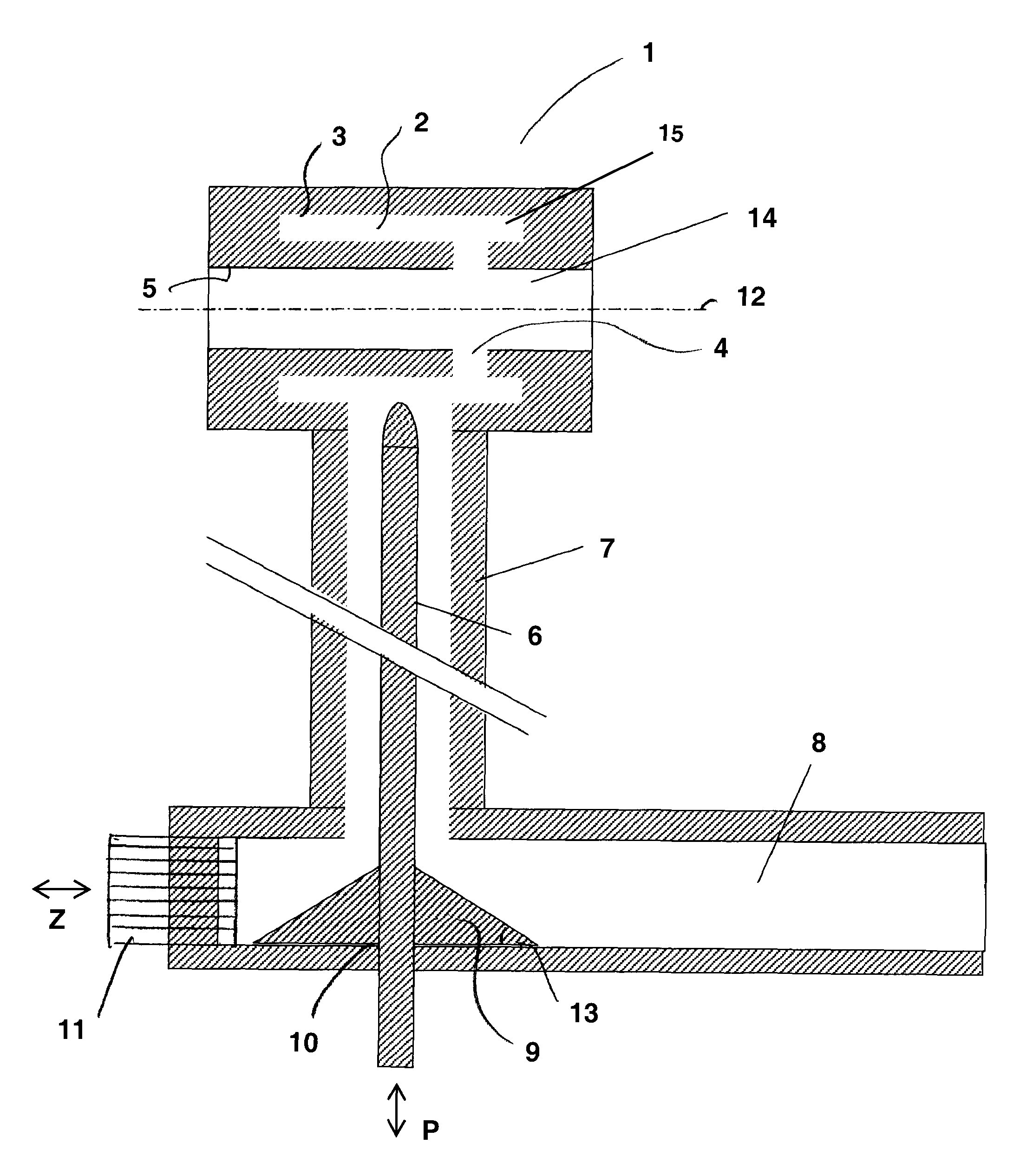
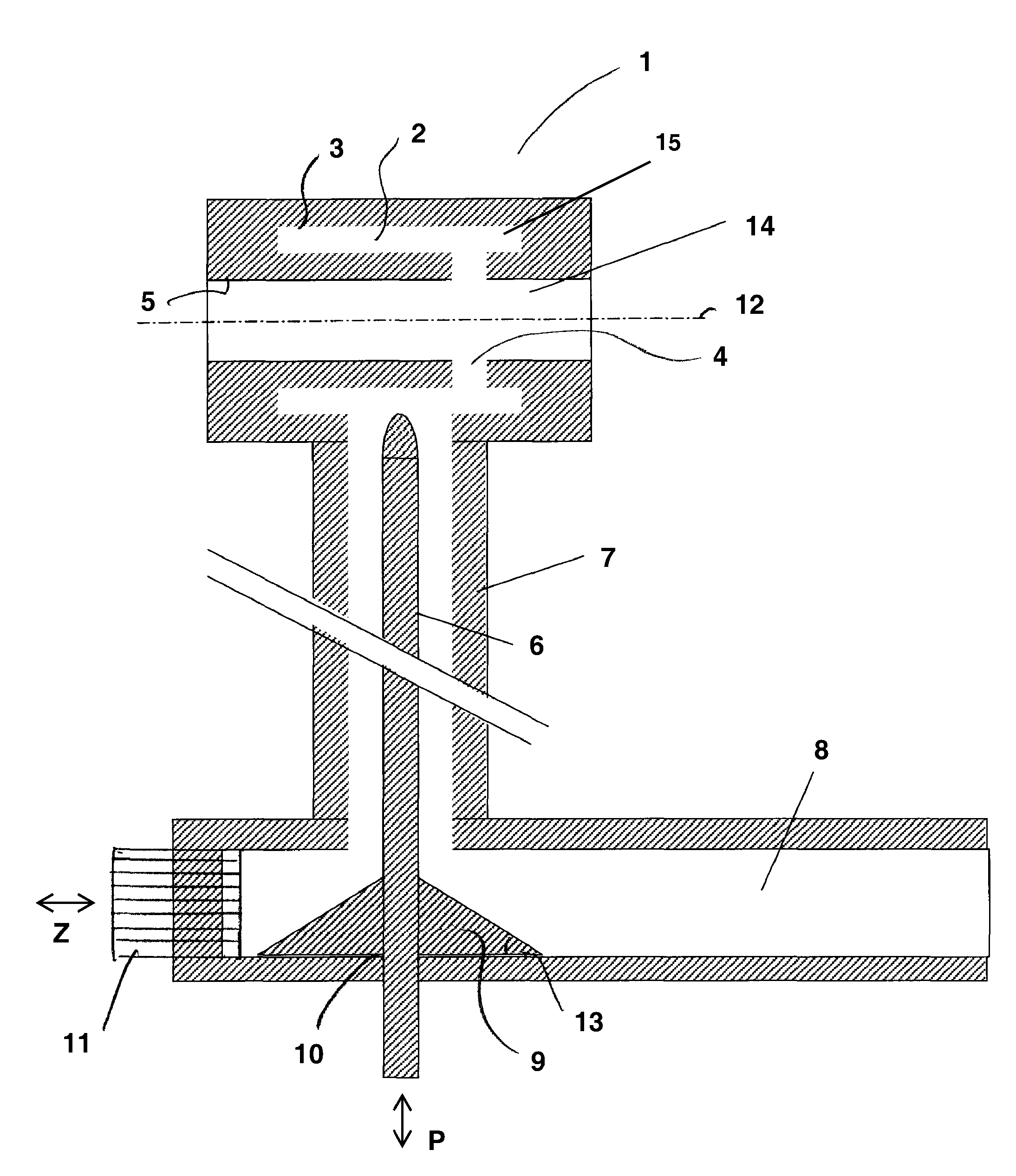
[0036]The present invention will now be explained in more detail with reference to the , which depicts an exemplary embodiment of the present invention. As will be appreciated by those having ordinary skill in the art, this FIGURE is a schematic representation, which is not necessarily drawn to scale. This invention may be embodied in many different forms and should not be construed as limited to the embodiments set forth herein. The embodiments disclosed are provided to convey the scope of the invention to those having skill in the relevant art.

[0037]In the FIGURE, the apparatus for carrying out a plasma chemical vapor deposition (PCVD) process is schematically indicated at 1. The apparatus 1 includes an internal guide or antenna 6, which is at least partially positioned in a coaxial waveguide 7. The antenna 6 is movable along a longitudinal axis in the coaxial waveguide 7 (i.e., in the direction indicated by the arrow P). The antenna 6 terminates in a resonant cavity 2.

[0038]A res...


PUM

PropertyMeasurementUnit
angleaaaaaaaaaa
angleaaaaaaaaaa
angleaaaaaaaaaa

Abstract

The present invention relates to an apparatus for carrying out a plasma chemical vapor deposition process by which one or more layers of doped or undoped silica can be deposited on the interior of an elongated glass substrate tube. The present invention further relates to a method for manufacturing an optical fiber using such an apparatus.

Description

CROSS-REFERENCE TO PRIORITY APPLICATION[0001]This application hereby claims the benefit of pending Dutch Application No. 1032015 (filed Jun. 16, 2006, at the Dutch Patent Office), which is hereby incorporated by reference in its entirety.FIELD OF THE INVENTION[0002]The present invention relates to an improved apparatus for performing plasma chemical vapor deposition (PCVD) by which one or more layers of doped or undoped silica can be deposited on the interior of an elongated glass substrate tube. The present invention further relates to methods of making an optical fiber using this apparatus.BACKGROUND OF THE INVENTION[0003]Microwave-enhanced chemical vapor deposition techniques are known in the art.[0004]For instance, U.S. Pat. No. 5,223,308 (Doehler) relates to a microwave-assisted deposition apparatus that comprises a microwave generator and a rectangular microwave waveguide that are employed to provide an electromagnetic field of intense microwave energy in a space in which an e...

Claims


Application Information

Patent Timeline
Patent Type & Authority Patents(United States)
IPC IPC(8): H05B31/26
CPCC03B37/0183C03B2201/12C03B2201/31
Inventor HARTSUIKER, JOHANNES ANTOONKORSTEN, MARCOVAN STRALEN, MATTHEUS JACOBUS NICOLAASDECKERS, ROB HUBERTUS MATHEUS
Owner DRAKA COMTEQ BV
Why Eureka
Try Eureka