Single photon absorption all-optical modulator in silicon

a technology of all-optical modulators and silicon, applied in non-linear optics, instruments, optics, etc., can solve the problems of severe limitations, requiring extremely high (5 w) peak optical power levels to achieve modulation, and weak effects both ways

Inactive Publication Date: 2010-07-20
CALIFORNIA INST OF TECH
View PDF1 Cites 43 Cited by
  • Summary
  • Abstract
  • Description
  • Claims
  • Application Information

AI Technical Summary

Problems solved by technology

Both effects are weak in silicon, and require extremely high (˜5 W) peak optical power levels to achieve modulation.
This approach has severe limitations.
Because of the disparate wavelengths for gate and signal, these devices cannot be cascaded into circuits that require feedback.

Method used


Image

  • Single photon absorption all-optical modulator in silicon
  • Single photon absorption all-optical modulator in silicon
  • Single photon absorption all-optical modulator in silicon

Examples


Embodiment Construction

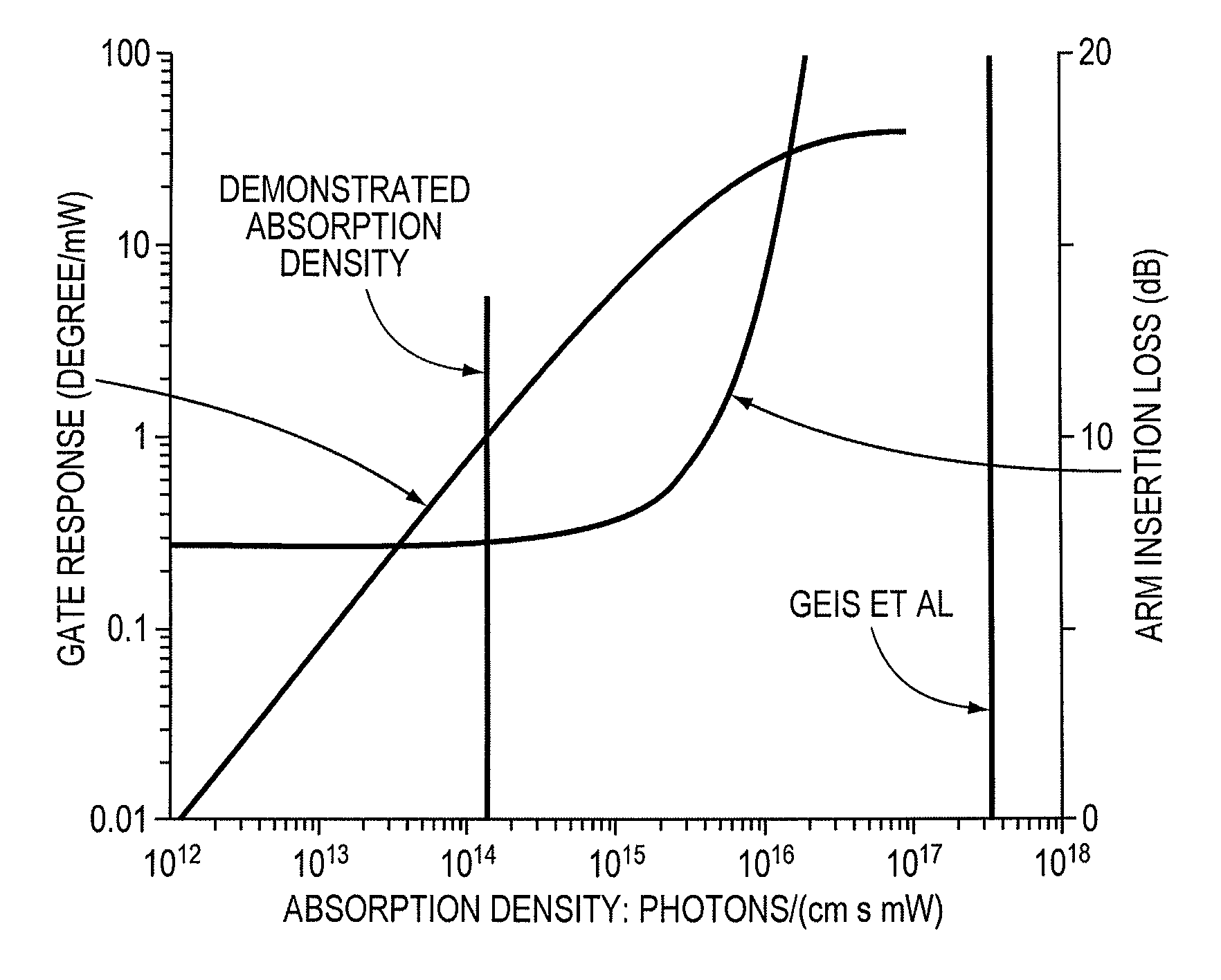
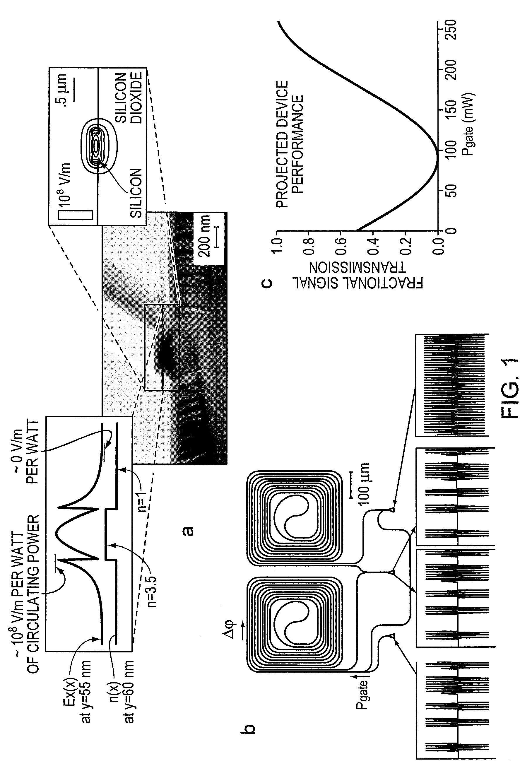
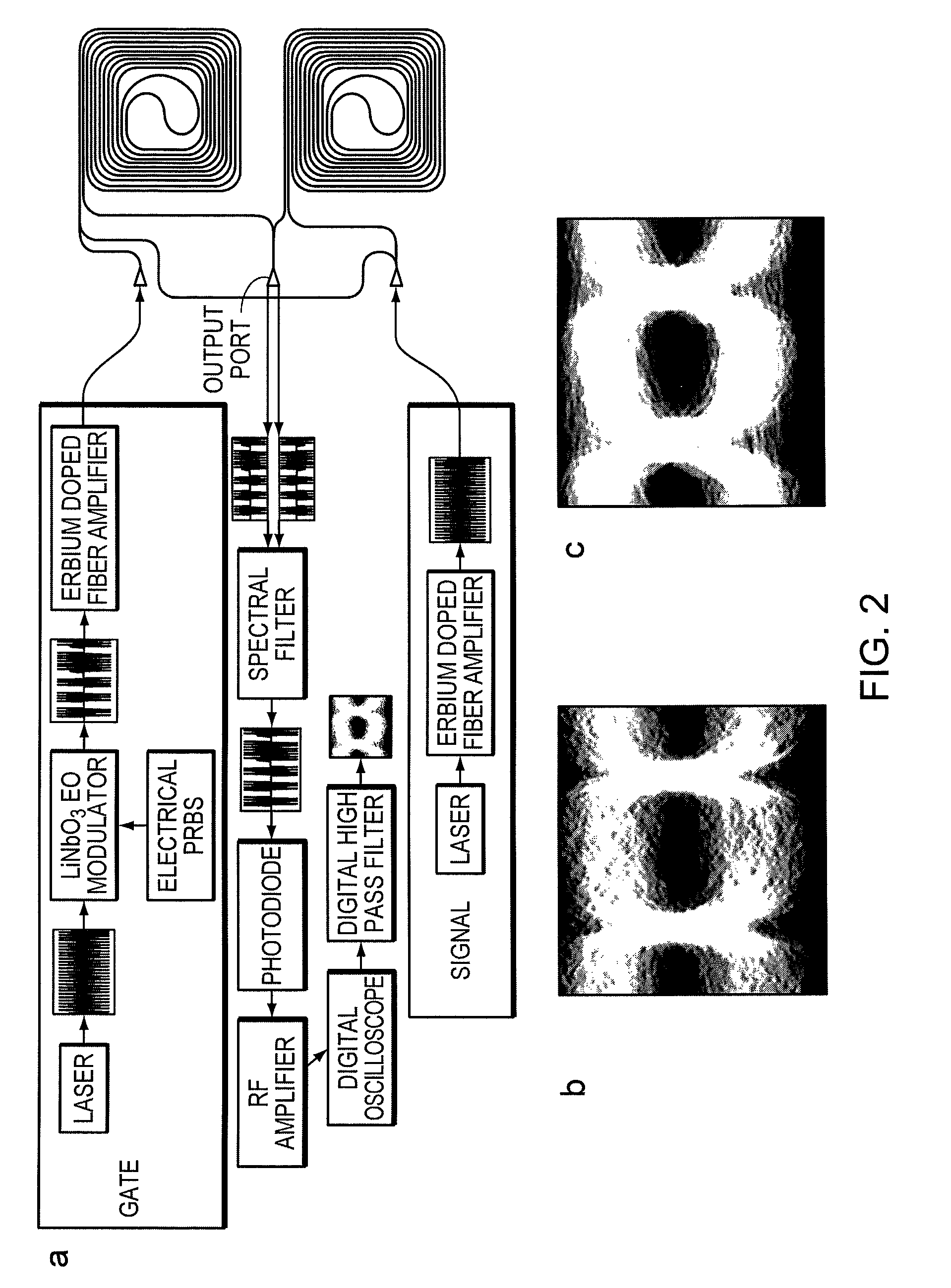
[0024]Because silicon has a bandgap of 1.12 eV, it is an ideal material platform for near-infrared integrated optical circuits. Electrically driven modulation and an optically pumped silicon laser have been previously demonstrated. For all-optical signal processing applications, low-power all-optical modulation is very useful and would represent an appreciable advance. Applications that are contemplated include optical buffering, all-optical wavelength conversion, and all-optical computation. Silicon is also a useful material because of its low cost as compared to many other semiconductors, and because it has a very well developed and well understood processing technology. Nevertheless, other semiconductor materials might in principle be used instead of silicon in a single-photon absorption device. For some optical wavelengths, other materials might be advantageous as compared to silicon.

[0025]We describe an all-optical Mach-Zehnder modulator based on a single-photon absorption (SPA...


PUM

PropertyMeasurementUnit
lengthaaaaaaaaaa
frequencyaaaaaaaaaa
quantum efficiencyaaaaaaaaaa

Abstract

A single-photon absorption all-optical modulator, systems employing the same, and methods of making and using the same. An illustrative example is provided based on silicon semiconductor technology that employs rectangular waveguides. In some embodiments, it is observed that the waveguides operate with an absorption density of less than 1017 cm−1s−1mW−1 to provide a single-photon absorption operation mode.

Description

CROSS-REFERENCE TO RELATED APPLICATIONS[0001]This application claims priority to and the benefit of U.S. provisional patent application Ser. No. 60 / 998,490, filed Oct. 11, 2007, which application is incorporated herein by reference in its entirety.STATEMENT REGARDING FEDERALLY FUNDED RESEARCH OR DEVELOPMENT[0002]The U.S. Government has certain rights in this invention pursuant to Grant No. HR0011-04-1-0054 awarded by DARPA.FIELD OF THE INVENTION[0003]The invention relates to all-optical modulators in general and particularly to a silicon all-optical modulator that employs single photon absorption.BACKGROUND OF THE INVENTION[0004]All-optical, low-power modulation is a major goal in photonics. Because of their high mode-field concentration and ease of manufacturing, nanoscale silicon waveguides offer an intriguing platform for photonics. To the best knowledge and belief of the inventors, all-optical modulators built with silicon photonic circuits have relied on either two-photon absor...

Claims


Application Information

Patent Timeline
Patent Type & Authority Patents(United States)
IPC IPC(8): G02F1/035
CPCG02F1/3515G02F1/365G02F1/3517G02F2201/063
Inventor BAEHR-JONES, TOMHOCHBERG, MICHAEL J.SCHERER, AXEL
Owner CALIFORNIA INST OF TECH
Why Eureka
Try Eureka