Photolithography with optical masks having more transparent features surrounded by less transparent features

a technology of optical masks and transparent features, applied in the field of photolithography, can solve the problems of reducing the size of dark areas, corresponding to opaque features, and reducing the contrast between dark and light areas,

Active Publication Date: 2010-08-10
PROMOS TECH INC
View PDF3 Cites 19 Cited by
  • Summary
  • Abstract
  • Description
  • Claims
  • Application Information

AI Technical Summary

Problems solved by technology

The areas corresponding to the opaque features can thus be undesirably illuminated, reducing the contrast between the dark and light areas and / or reducing the dark areas' sizes.
The clear features inside the opaque features are not printed, i.e. are projected onto dark areas of the photoresist, as the size of these clear features cannot be resolved by the projection system.

Method used


Image

  • Photolithography with optical masks having more transparent features surrounded by less transparent features
  • Photolithography with optical masks having more transparent features surrounded by less transparent features
  • Photolithography with optical masks having more transparent features surrounded by less transparent features

Examples


Embodiment Construction

[0014]The embodiments described in this section illustrate but do not limit the invention. The invention is defined by the appended claims.

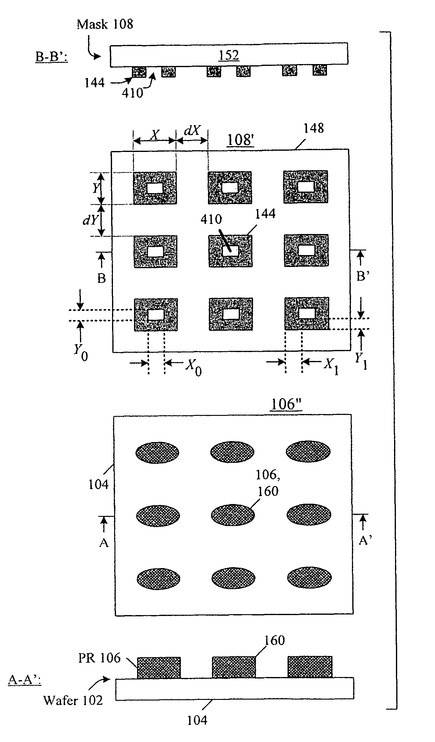
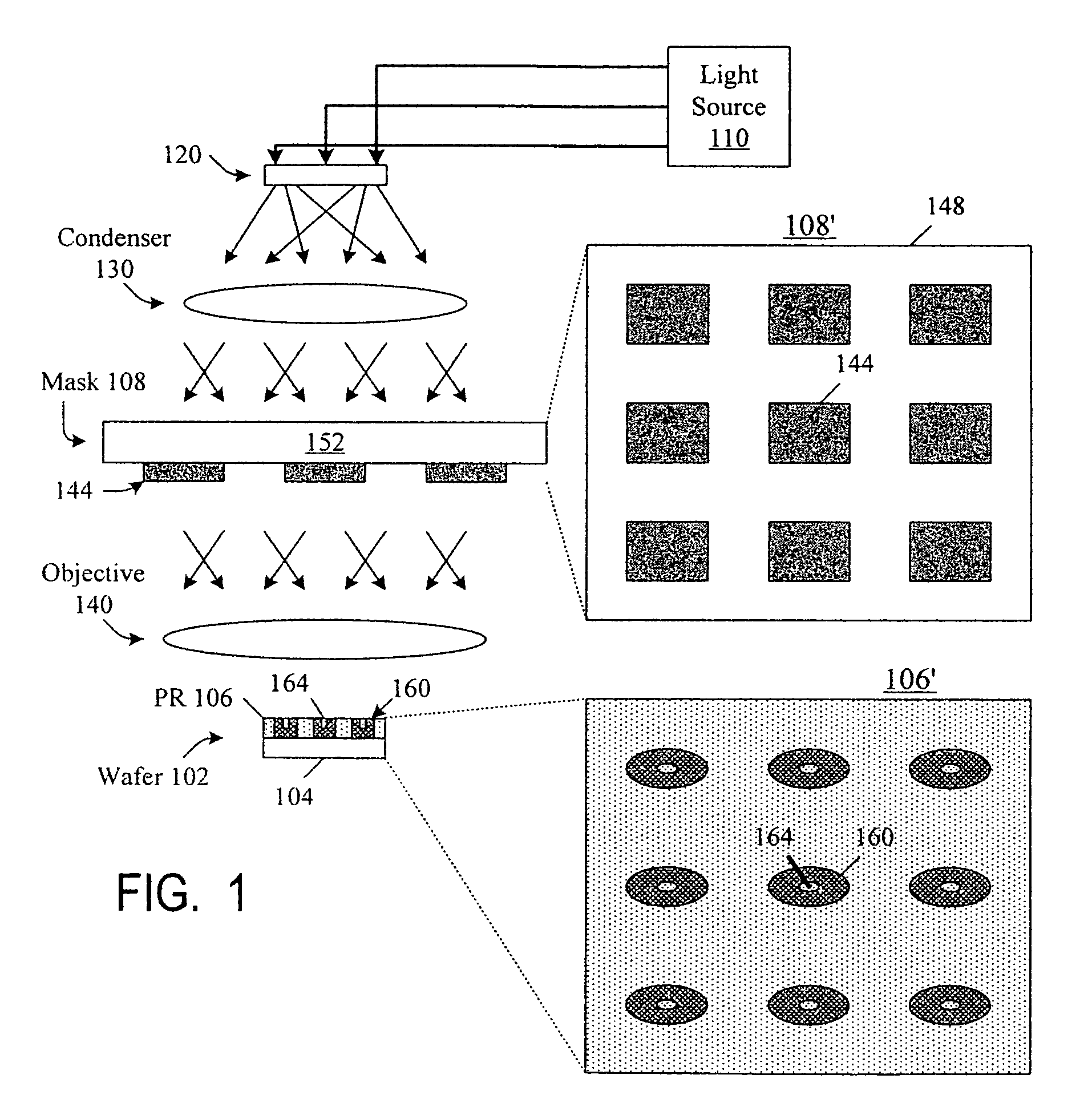
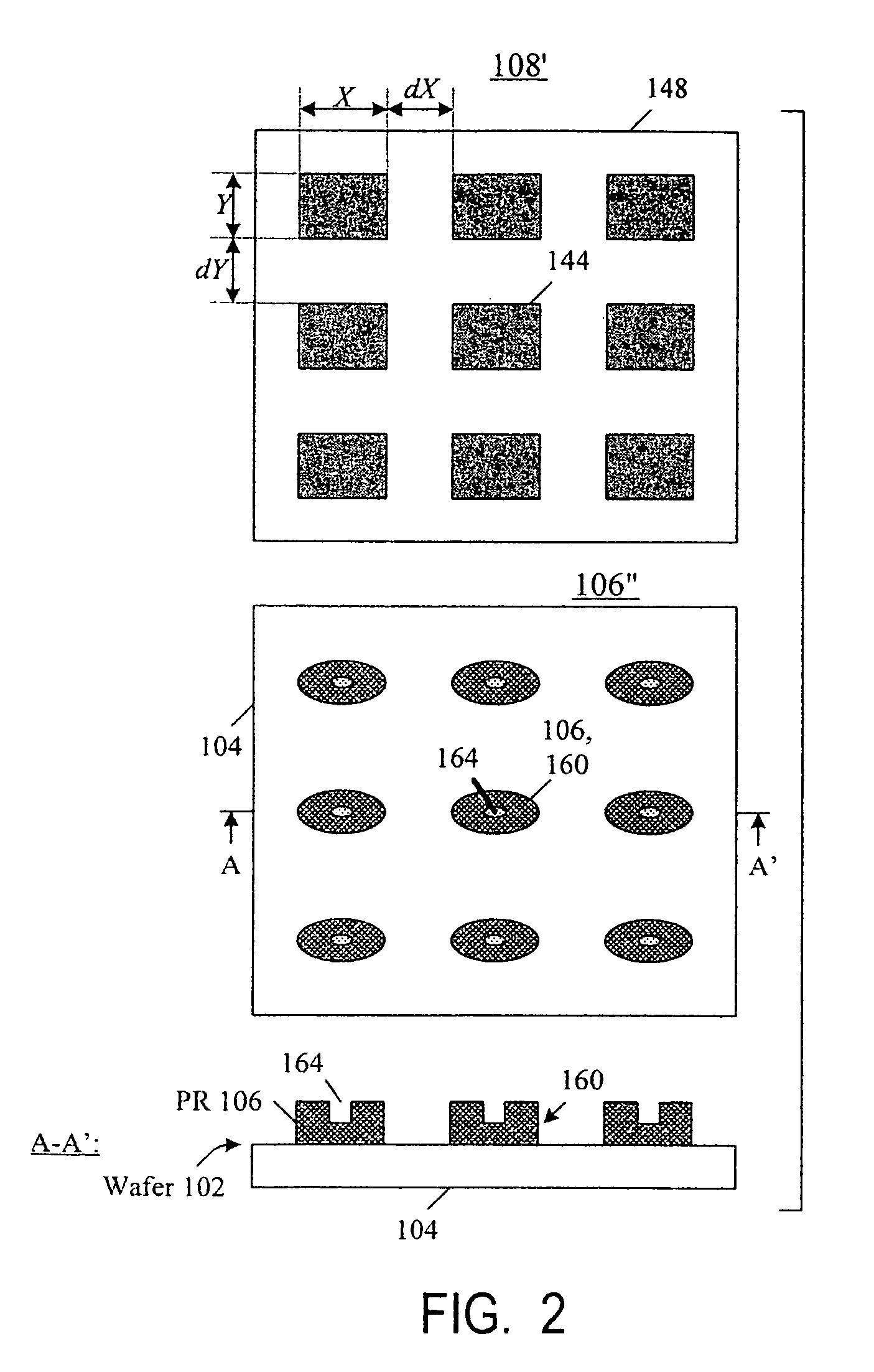
[0015]FIG. 1 is a side view of an exemplary photolithographic exposure system used to form an illumination pattern on a wafer 102 including a substrate 104 covered with a photoresist layer 106. The system is projection type, with optical mask 108 being at a distance from the wafer. Coherent light emitted by a laser light source 110 passes through an illumination pupil 120 positioned in the focal plane of a condenser lens 130. The light emerging from pupil 120 is coherent or partially coherent. Condenser lens 130 concentrates the light on the mask 108. Objective lens 140 images the pattern of mask 108 onto the photoresist 106. Objective 140 may also shrink the mask pattern (by a factor S of four or five for example). A suitable exposure system is type ASML XT 1250 (Trademark) available from ASML Holding N.V., De Run 6501, 5504 DR Veldhoven, The Ne...


PUM

PropertyMeasurementUnit
light wavelengthaaaaaaaaaa
wavelengthaaaaaaaaaa

Abstract

In photolithographic exposure, a feature (144) of an optical mask is projected onto a dark area (160). The light intensity inside the dark area is reduced by providing a non-printable clear cutout (410) inside the feature. The optical mask has the same optical pathlength outside the feature (144) adjacent to the entire outer boundary of the feature as at the cutout, the optical pathlength being measured along the optical mask's thickness.

Description

BACKGROUND OF THE INVENTION[0001]The present invention relates to photolithography.[0002]In a photolithographic exposure process, a wafer surface is coated with photoresist, and the photoresist is illuminated by light passing through an optical mask having a pattern of clear and opaque features. These features define an illumination pattern of light and dark areas on the photoresist surface. At the light areas, the photoresist becomes more soluble (if positive) or less soluble (if negative) in a developer solution. The wafer is then placed into the developer solution to dissolve the soluble portions of the photoresist. The remaining photoresist provides a photoresist mask used in subsequent processing (e.g. etching, deposition, ion implantation, etc.).[0003]In non-contact exposure, the optical mask is held at a distance from the photoresist surface to avoid mask damage. Due to bending of light rays, the pattern of light and dark areas in the photoresist does not always correspond to...

Claims


Application Information

Patent Timeline
Patent Type & Authority Patents(United States)
IPC IPC(8): G03F1/00G03C5/00
CPCG03F1/144G03F1/36G03F7/70441G03F1/50
Inventor ZHANG, FENGHONGZHANG, XINYUXU, JIAN
Owner PROMOS TECH INC
Why Eureka
Try Eureka