Lead frame based, over-molded semiconductor package with integrated through hole technology (THT) heat spreader pin(s) and associated method of manufacturing

a technology of semiconductor packaging and heat spreader pin, which is applied in the direction of individual semiconductor device testing, semiconductor/solid-state device testing/measurement, instruments, etc., can solve the problems of increasing the thermal resistivity of the heat path, and conventional approaches to dissipate heat do not address the problem of high thermal resistivity generated

Active Publication Date: 2010-08-10
NXP USA INC
View PDF15 Cites 9 Cited by
  • Summary
  • Abstract
  • Description
  • Claims
  • Application Information

AI Technical Summary

Benefits of technology

[0035]Benefits, other advantages, and solutions to problems have been described above with regard to specific embodiments. For example, the disclosed lead frame based semiconductor package structures provide an optimized thermal path within the package by reducing thermal resistance values within the intended heat path through the PCB onto the PCB backside (which features a large copper plane acting as a heat sink) by inserting a heat conducting or spreading pin structure into the thermal vias of PCB. In addition, typical assembly issues (i.e., solder voiding) which may limit the package on-board performance can be eliminated, and the heat spreader pins allow the package and PCB to be self-aligned during PCB assembly. However, the benefits, advantages, solutions to problems, and any element(s) that may cause any benefit, advantage, or solution to occur or become more pronounced are not to be construed as a critical, required, or essential feature or element of any or all the claims. As used herein, the terms “comprises,”“comprising,” or any other variation thereof, are intended to cover a non-exclusive inclusion, such that a process, method, article, or apparatus that comprises a list of elements does not include only those elements but may include other elements not expressly listed or inherent to such process, method, article, or apparatus.

Problems solved by technology

Thermal resistivity of the heat path can also be increased by typical assembly issues, such as solder voiding.
As shown in U.S. Patent Application Publication No. 2005 / 0110137, conventional approaches for dissipating heat do not address the issue of the high thermal resistivity generated by the thermal vias of the PCB.

Method used


Image

  • Lead frame based, over-molded semiconductor package with integrated through hole technology (THT) heat spreader pin(s) and associated method of manufacturing
  • Lead frame based, over-molded semiconductor package with integrated through hole technology (THT) heat spreader pin(s) and associated method of manufacturing
  • Lead frame based, over-molded semiconductor package with integrated through hole technology (THT) heat spreader pin(s) and associated method of manufacturing

Examples


Embodiment Construction

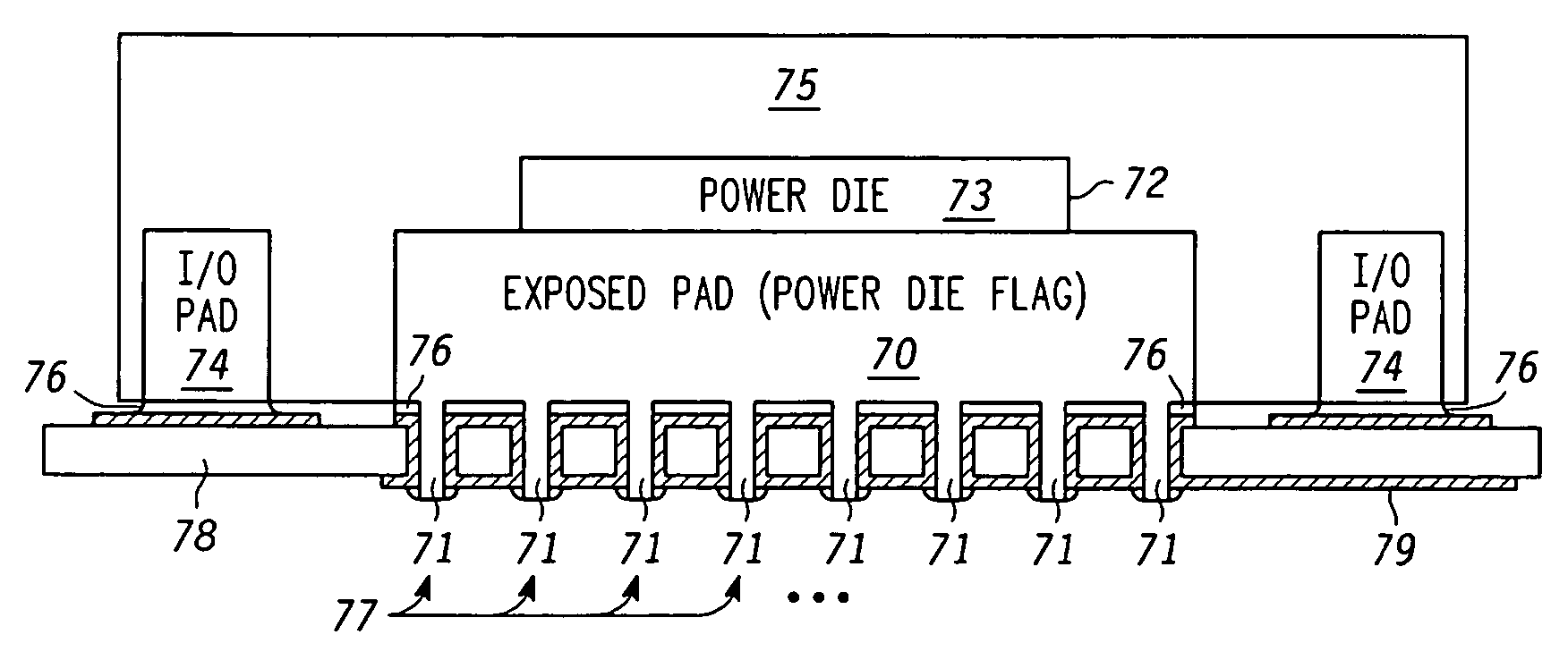
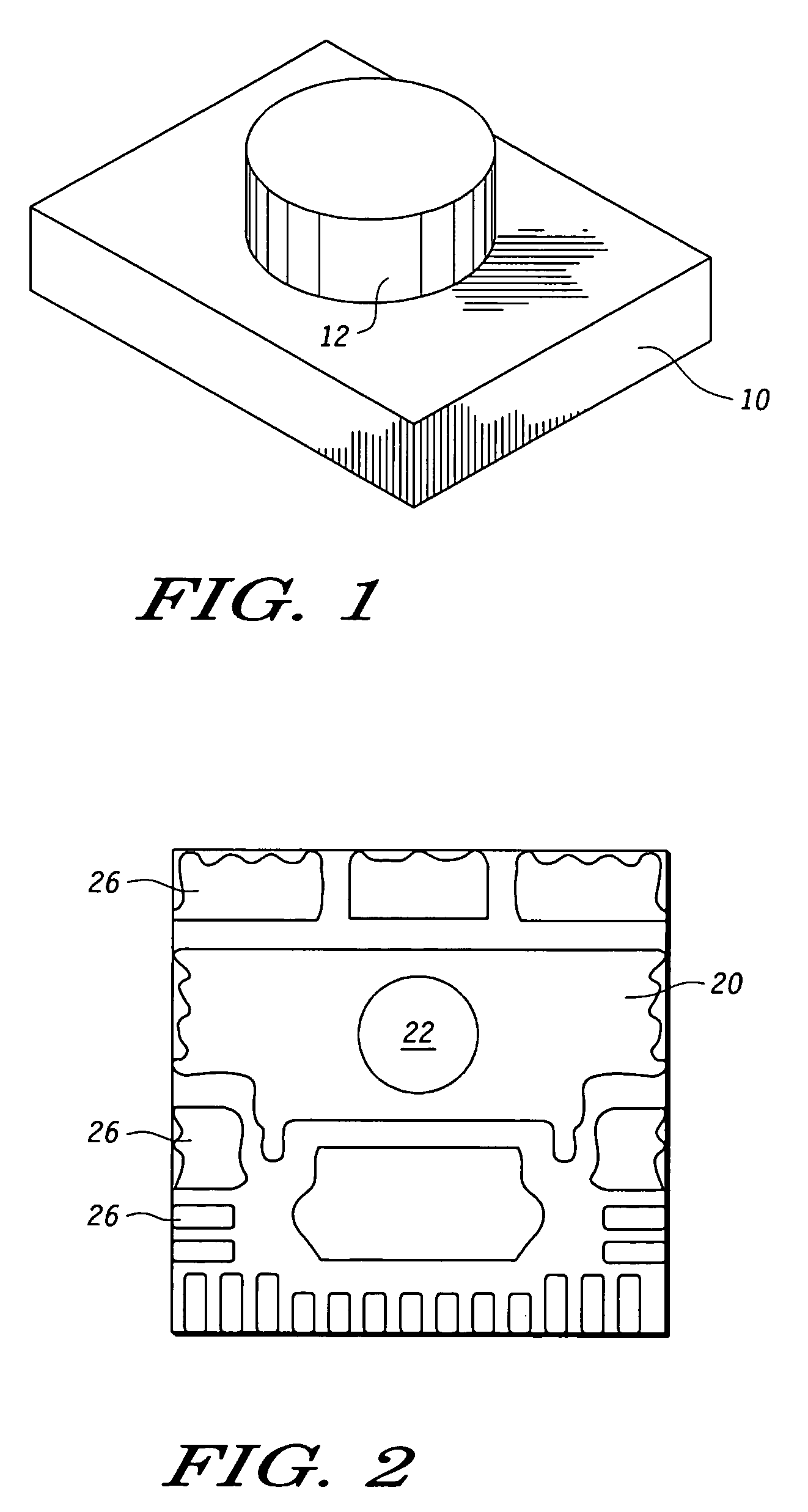
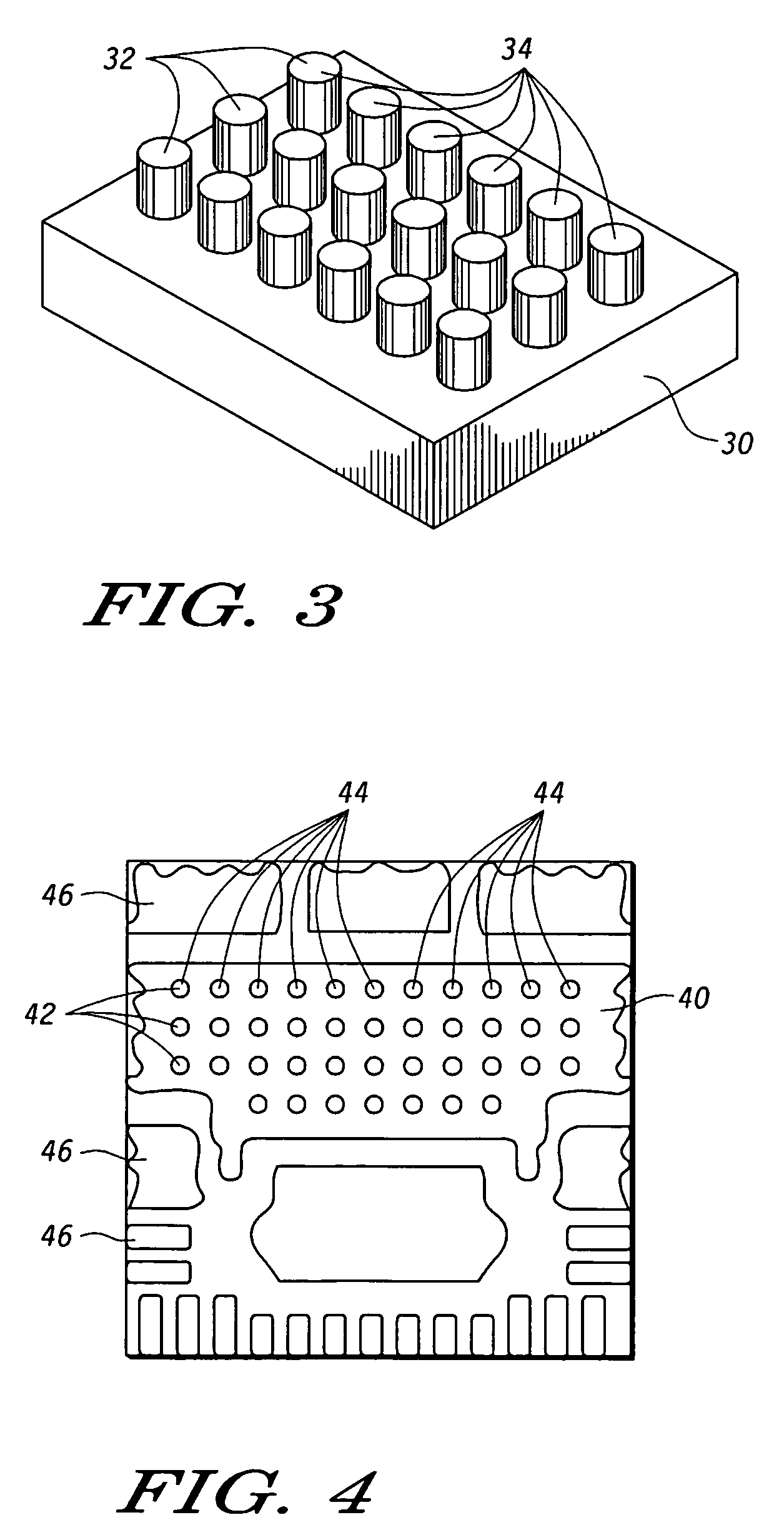
[0017]A method and apparatus are described for packaging a semiconductor device using a lead frame-based over-molded semiconductor package with one or more through hole technology (THT) heat spreader pin(s) on an exposed pad as a direct electrical and heat path having reduced resistance. By integrally forming or attaching the heat spreader pin(s) to an exposed die pad, a direct and short electrical and heat path is provided from the die attach pad to the package outside. The THT heat spreader pins may be manufactured in the lead frame manufacturing process, or may be pre-formed ahead of the actual package manufacturing process.

[0018]Various illustrative embodiments of the present invention will now be described in detail with reference to the accompanying figures. While various details are set forth in the following description, it will be appreciated that the present invention may be practiced without these specific details, and that numerous implementation-specific decisions may b...


PUM


Abstract

A method and apparatus are provided for manufacturing a lead frame based, over-molded semiconductor package (7) with an exposed pad or power die flag (70) having multiple integrated THT heat spreader pins (71) configured for insertion into one or more vias (77) formed in a printed circuit board (78). The through hole heat spreader pins (71) may be formed as an integral part of the exposed pad (52) or may be solidly connected with the exposed pad (62).

Description

BACKGROUND OF THE INVENTION[0001]1. Field of the Invention[0002]This invention relates to lead frame based semiconductor packages and a method of manufacturing the same. In one aspect, the present invention relates to a lead frame based over-molded semiconductor package with an exposed pad having an improved electrical and thermal path within the package as well as within the completed assembly of package and printed circuit board (PCB) or any other substrate material.[0003]2. Description of the Related Art[0004]Semiconductor packages with exposed pad (i.e., PQFN, QFN, HSOP, SOIC, QFP, TQFP, MO-188 etc.) provide a thermal path within the package to conduct heat from the integrated circuit die to the printed circuit board (PCB). After PCB assembly, the highest thermal resistance values within the intended heat path are induced by the thermal vias of PCB which lead through the PCB onto the PCB backside where a large copper plane acts as a heat sink. Thermal resistivity of the heat pat...

Claims


Application Information

Patent Timeline
Patent Type & Authority Patents(United States)
IPC IPC(8): H01L21/00
CPCH01L21/568H01L23/49568H01L24/97H01L23/3107H01L2924/10253H01L2224/48247H01L2924/01076H01L2924/01006H01L24/48H01L2224/48091H01L2224/97H01L2924/01015H01L2924/01029H01L2924/01033H01L2924/01042H01L2924/01047H01L2924/01082H01L2924/14H01L2924/00014H01L2224/85H01L2924/00H01L2924/181H01L2924/00012H01L2224/45099H01L2224/45015H01L2924/207H01L23/34
Inventor BAUER, ROBERTKOLBECK, ANTON
Owner NXP USA INC
Why Eureka
Try Eureka