Thin stacked interposer package

a technology of interposer package and stacking, which is applied in the direction of semiconductor devices, semiconductor/solid-state device details, electrical apparatus, etc., can solve the problems of limited and precious space on printed circuit boards, and existing solutions for stacking such as straddle mount laminate bga or stacked die tsop often do not meet form factor requirements

Active Publication Date: 2010-08-17
AMKOR TECH SINGAPORE HLDG PTE LTD
View PDF415 Cites 399 Cited by
  • Summary
  • Abstract
  • Description
  • Claims
  • Application Information

AI Technical Summary

Benefits of technology

[0010]In accordance with one embodiment of the present invention, there is provided a semiconductor package comprising a bottom semiconductor package substrate which is populated with one or more electronic components. The electronic component(s) of the bottom substrate are covered or encapsulated with a suitable mold compound which hardens into a package body of the semiconductor package. The package body is provided with one or more vias through the completion of lasering or similar drilling process, such via(s) providing access to one or more corresponding conductive contacts of the bottom substrate. These vias are either lined or at least partially filled with a conductive metal material. Subsequently, a top semiconductor package substrate (an interposer) which may optionally be populated with one or more electronic components is mounted to the package body and electrically connected to the conductive metal material within the via(s) of the package body.

Problems solved by technology

Even though semiconductor packages have been miniaturized, space on a printed circuit board remains limited and precious.
However, existing solutions for package stacking such as straddle mount laminate BGA or stacked die TSOP often do not meet form factor requirements.

Method used


Image

  • Thin stacked interposer package
  • Thin stacked interposer package
  • Thin stacked interposer package

Examples


first embodiment

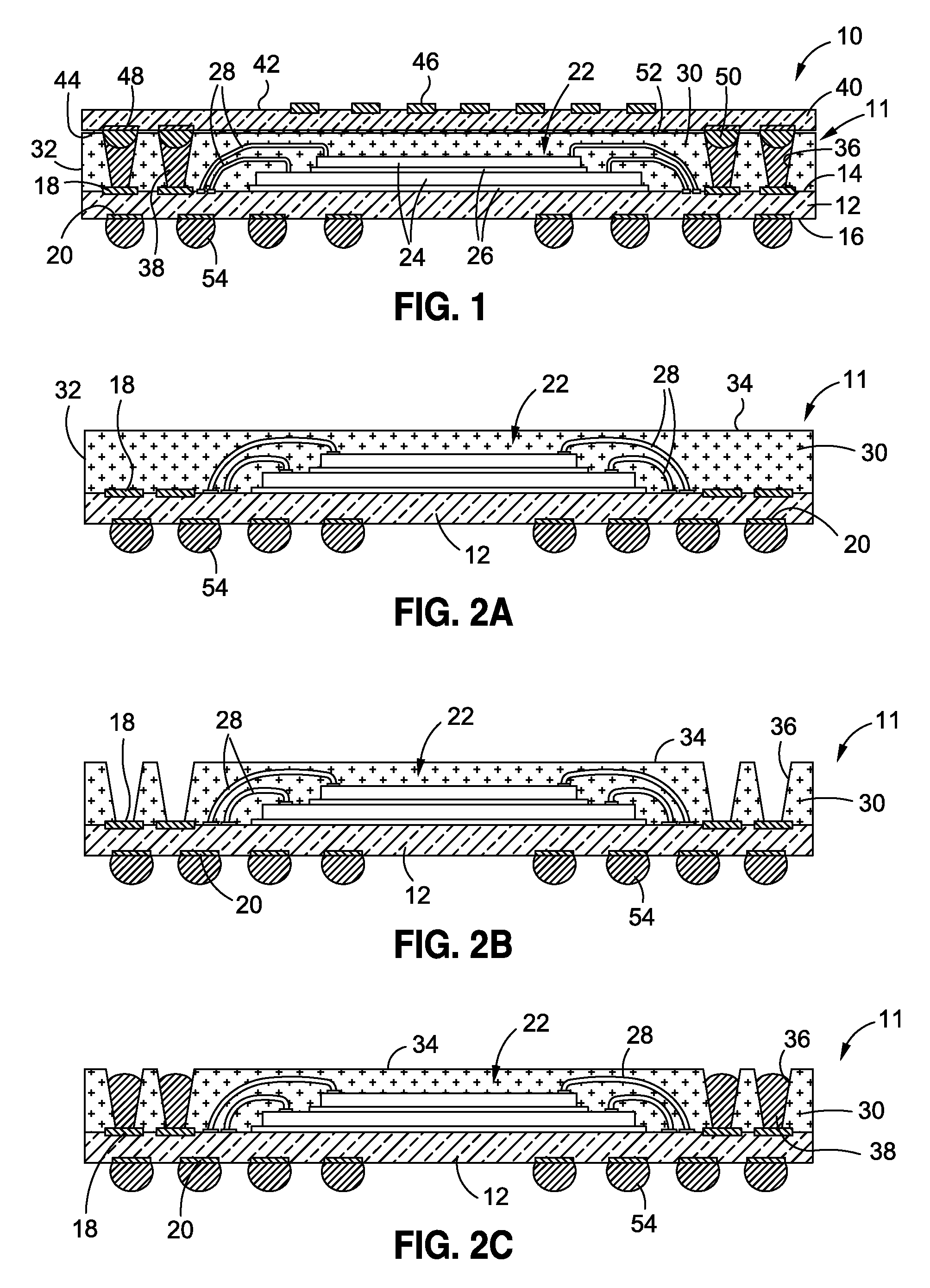
[0031]Referring now to the drawings wherein the showings are for purposes of illustrating various embodiments of the present invention only, and not for purposes of limiting the same, FIG. 1 depicts a semiconductor package 10 constructed in accordance with the present invention. The semiconductor package 10 comprises a bottom substrate assembly 11, which itself comprises a laminate bottom substrate 12 which has a generally quadrangular configuration defining four (4) peripheral edge segments. In addition, the bottom substrate 12 defines a generally planar top surface 14 and an opposed, generally planar bottom surface 16. Disposed on the top surface 14 is a plurality of top contacts 18 of the bottom substrate 12. In the bottom substrate 12, the top contacts 18 are typically disposed in relative close proximity to the peripheral edge segments defined by the bottom substrate 12. Formed on the bottom surface 16 of the bottom substrate 12 is a plurality of bottom contacts 20. Though not ...

second embodiment

[0039]Referring now to FIG. 4, there shown a semiconductor package 10a constructed in accordance with the present invention. The semiconductor package 10a is substantially similar in construction to the semiconductor package 10 described above, with the sole distinction between the semiconductor packages 10, 10a lying in the semiconductor package 10a including only a single semiconductor die 24a mounted and electrically connected to the bottom substrate 12a of the bottom substrate assembly 11a. The inclusion of the single semiconductor die 24a in the semiconductor package 10a is in contrast to the die stack 22 having the stacked semiconductor dies 24 which is included in the semiconductor package 10.

third embodiment

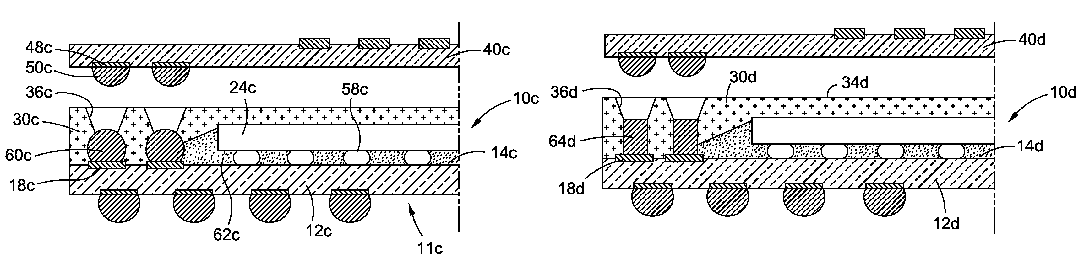
[0040]Referring now to FIGS. 5 and 6, there shown a semiconductor package 10b constructed in accordance with the present invention. The semiconductor package 10b is substantially similar to the semiconductor package 10a shown in FIG. 4, except that the single semiconductor die 24b of the semiconductor package 10b is electrically connected to the bottom substrate 12b through the use of a flip-chip type connection, as opposed to the use of the conductive wires 28a used in conjunction with the semiconductor die 24a in the semiconductor package 10a. More particularly, in the semiconductor package 10b, conductive posts 56b which may be made of copper or a similar, suitable conductive material are used to electrically connect pads or terminals of the semiconductor die 24b to corresponding pads or traces of the bottom substrate 12b which are in turn electrically connected to the top contacts 18b thereof in a prescribed pattern or arrangement. Those of ordinary skill in the art will recogni...


PUM


Abstract

The present invention comprises a semiconductor package comprising a bottom semiconductor package substrate which is populated with one or more electronic components. The electronic component(s) of the bottom substrate are covered or encapsulated with a suitable mold compound which hardens into a package body of the semiconductor package. The package body is provided with one or more vias through the completion of laser drilling process, such via(s) providing access to one or more corresponding conductive contacts of the bottom substrate. These vias are either lined or partially filled with a conductive metal material. Subsequently, a top semiconductor package substrate (which may optionally be populated with one or more electronic components) is mounted to the package body and electrically connected to the conductive metal within the via(s) of the package body.

Description

CROSS-REFERENCE TO RELATED APPLICATIONS[0001]Not ApplicableSTATEMENT RE: FEDERALLY SPONSORED RESEARCH / DEVELOPMENT[0002]Not ApplicableBACKGROUND OF THE INVENTION[0003]1. Field of the Invention[0004]The present invention relates generally to integrated circuit chip package technology and, more particularly, to a semiconductor package which is configured in a manner wherein two complimentary laminate substrate elements (i.e., a bottom element and a top element) are electrically connected to each other subsequent to one or both of the substrate elements being populated with various electronic components. Further in accordance with the present invention, there is provided a stacked wafer level chip scale package (WLCSP).[0005]2. Description of the Related Art[0006]Semiconductor dies are conventionally enclosed in plastic packages that provide protection from hostile environments and enable electrical interconnection between the semiconductor die and an underlying substrate such as a prin...

Claims


Application Information

Patent Timeline
Patent Type & Authority Patents(United States)
IPC IPC(8): H01L23/48H01L29/40H01L23/52
CPCH01L23/3128H01L25/0657H01L25/105H01L24/16H01L24/45H01L24/48H01L2224/16225H01L2224/32145H01L2224/32225H01L2224/45124H01L2224/45144H01L2224/45147H01L2224/48091H01L2224/48095H01L2224/48227H01L2224/73204H01L2224/73265H01L2225/06517H01L2225/06541H01L2924/01078H01L2924/01079H01L2924/078H01L2924/14H01L2924/15311H01L2924/1532H01L2924/15331H01L2924/18161H01L2924/00014H01L2924/15321H01L2225/1023H01L2225/1041H01L2225/1058H01L2924/00H01L2924/00012H01L2924/01013H01L2924/01047H01L24/73H01L2924/00011H01L2924/181H01L2924/1815H01L2224/0401
Inventor BERRY, CHRISTOPHER J.SCANLAN, CHRISTOPHER M.
Owner AMKOR TECH SINGAPORE HLDG PTE LTD
Why Eureka
Try Eureka