Unlock instant, AI-driven research and patent intelligence for your innovation.

Method for manufacturing a semiconductor device by selective etching

a selective etching and semiconductor technology, applied in the direction of semiconductor devices, basic electric elements, electrical appliances, etc., can solve the problem of difficult to form fine patterns in the peripheral circuit region, and achieve the effect of improving the data processing speed of the semiconductor device and increasing the efficiency of the devi

Inactive Publication Date: 2010-08-24
SK HYNIX INC
View PDF6 Cites 0 Cited by
  • Summary
  • Abstract
  • Description
  • Claims
  • Application Information

AI Technical Summary

Benefits of technology

The invention provides a method for manufacturing a semiconductor device that ensures a sufficient process margin to enable the formation of a fine pattern in a peripheral circuit region. The method includes sequentially forming a hard mask layer and a first anti-reflective layer over an etching target layer, selectively etching the first anti-reflective layer to expose the hard mask layer in the isolation pattern region, forming a second anti-reflective layer of a preset thickness over the first anti-reflective layer and the hard mask layer in the isolation pattern region, and selectively etching the second anti-reflective layer, the first anti-reflective layer, and the hard mask layer, thereby forming a hard mask pattern and over-etching the second anti-reflective layer in the isolation pattern region. The method improves the data processing speed of a semiconductor device and increases device efficiency.

Problems solved by technology

In reality, however, an isolation pattern in the peripheral circuit region has a short process margin, compared with a dense pattern in a cell region, so it is difficult to form a fine pattern in the peripheral circuit region.
This difficulty arises during a pattern formation process in which a broad area of the isolation pattern in the peripheral circuit region is etched.

Method used


Image

  • Method for manufacturing a semiconductor device by selective etching
  • Method for manufacturing a semiconductor device by selective etching
  • Method for manufacturing a semiconductor device by selective etching

Examples


Embodiment Construction

[0016]Hereinafter, the invention is described in detail with reference to the accompanying drawings so that those skilled in the art can easily carry out the invention.

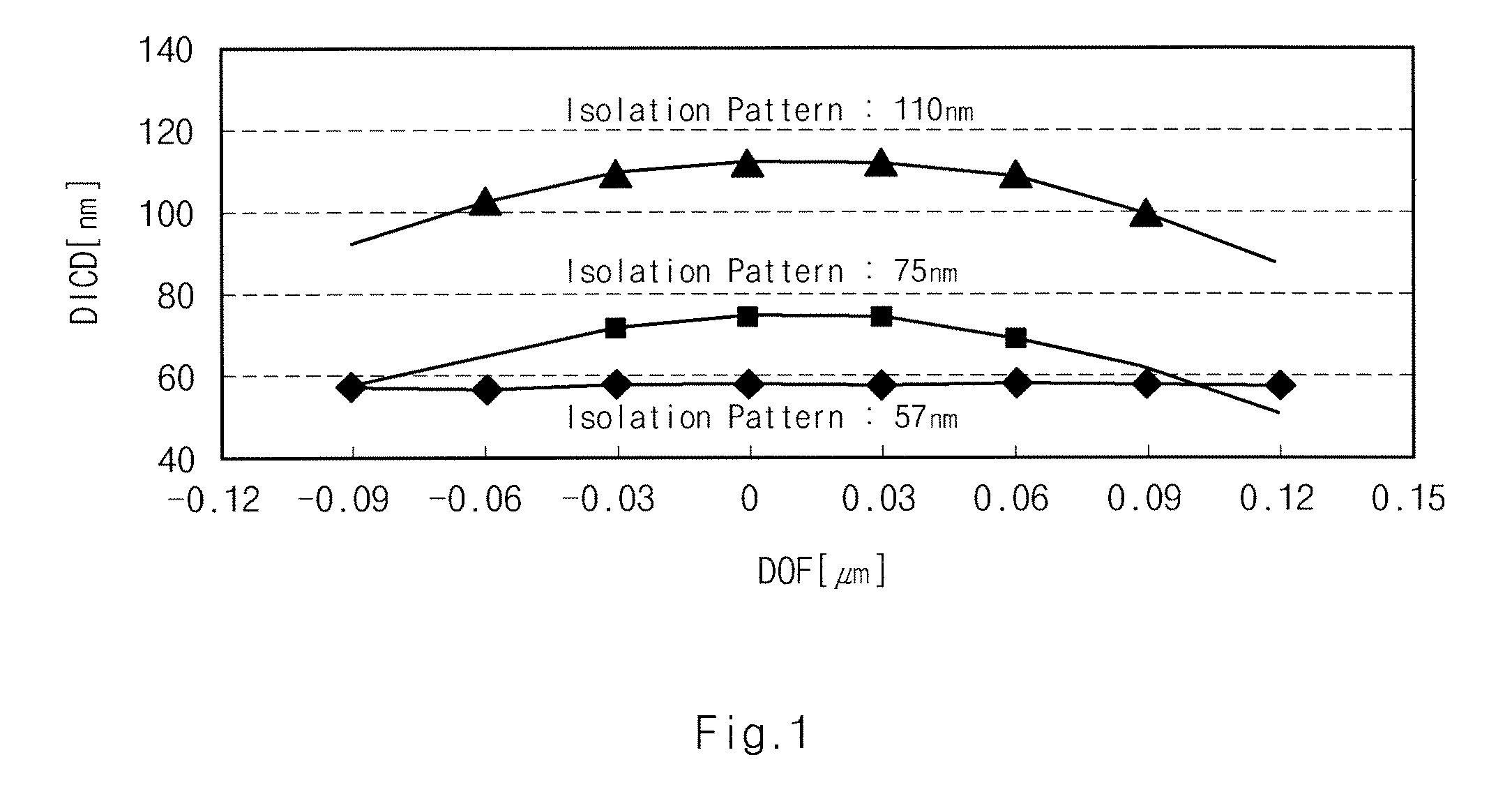
[0017]FIG. 1 is a graph showing the relation between develop inspection critical dimension (DICD) and depth of focus (DOF) of a dense line with a line width of 57 nm, an isolation line pattern with a line width of 75 nm, and an isolation line pattern with a line width of 110 nm, respectively.

[0018]Referring to the graph, the isolation line pattern with a line width of 75 nm has a comparatively smaller DOF margin than that of the dense line pattern with a line width of 57 nm.

[0019]Meanwhile, the isolation line pattern with a line width of 110 nm, which is relatively larger than the dense line pattern with a line width of 57 nm, exhibits an improved DOF margin compared to the isolation line pattern with a line width of 75 nm.

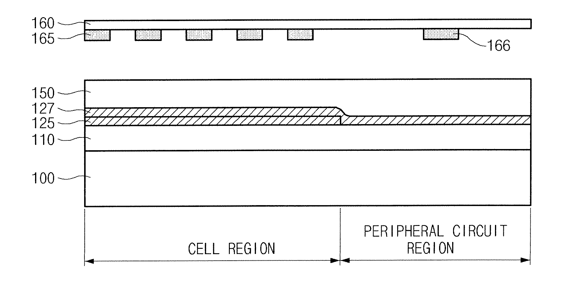
[0020]As mentioned earlier, to ensure a DOF margin of an isolation pattern formed in a periphera...


PUM


Abstract

A method of manufacturing a semiconductor device according to the invention is an effective technique for ensuring a sufficient process margin and enabling the formation of a fine pattern in a peripheral circuit region. The method includes forming an anti-reflective layer with a varying thickness in a peripheral circuit region and a cell region, and then over-etching the anti-reflective layer in the peripheral circuit region. The method is capable of improving the data processing speed of a semiconductor device and therefore increases the device efficiency.

Description

CROSS-REFERENCE TO RELATED APPLICATION[0001]The priority of Korean patent application number 10-2006-0099912, filed on Oct. 13, 2006, the entire disclosure of which is incorporated herein by reference, is claimed.BACKGROUND OF THE INVENTION[0002]The invention relates generally to a semiconductor device and a method for manufacturing a semiconductor device. More specifically, the invention relates to a technique that is effective for ensuring a sufficient process margin to enable the formation of a fine pattern in a peripheral circuit region. The invention includes forming an anti-reflective layer with a varying thickness in a peripheral circuit region as compared to a cell region, and then over-etching the anti-reflective layer in the peripheral circuit region. The invention is capable of improving the data processing speed of a semiconductor device to thereby increase the device efficiency.[0003]With trends in size reduction according to the decreasing design rule of DRAM processes...

Claims


Application Information

Patent Timeline
Patent Type & Authority Patents(United States)
IPC IPC(8): H01L21/311
CPCH01L21/0276H01L21/0337H01L21/3086H01L27/10894H10B12/09H01L21/31144
Inventor PARK, SA RO HAN
Owner SK HYNIX INC