
Electrical fuse, semiconductor device having the same, and method of programming and reading the electrical fuse

a technology of electrical fuse and semiconductor device, applied in the field of electrical fuse, can solve the problems of deteriorating reliability of the repair process, defective or good semiconductor chip classification, etc., and achieve the effect of maximizing blowing efficiency

Active Publication Date: 2010-09-07
SAMSUNG ELECTRONICS CO LTD
View PDF20 Cites 2 Cited by
  • Summary
  • Abstract
  • Description
  • Claims
  • Application Information

AI Technical Summary

Benefits of technology

[0012]An exemplary embodiment of the present invention provides an electrical fuse that can maximize blowing efficiency.
[0013]An exemplary embodiment of the present invention provides a semiconductor device having an electrical fuse that can maximize blowing efficiency.
[0014]An exemplary embodiment of the present invention provides a method of programming and reading an electrical fuse that can improve the reliability of a repair process.
[0015]In an aspect of the present invention, an electrical fuse is used for maximizing blowing efficiency. The electrical fuse includes first and second anodes disposed apart from each other. A cathode is interposed between the first and second anodes. A first fuse link couples the first anode to the cathode, and a second fuse link couples the second anode to the cathode.
[0019]In an aspect of the present invention, a semiconductor device has an electrical fuse for maximizing blowing efficiency. The semiconductor device includes a semiconductor substrate. First and second anodes are disposed apart from each other on the semiconductor substrate. A cathode is interposed between the first and second anodes. A first fuse link couples the first anode to the cathode, and a second fuse link couples the second anode to the cathode. First and second interconnections are electrically connected to the first and second anodes, respectively. A third interconnection is electrically connected to the cathode.

Problems solved by technology

As a result, the semiconductor chips are classified as either defective or good.
As a result, the reliability of the repair process deteriorates.

Method used


Image

  • Electrical fuse, semiconductor device having the same, and method of programming and reading the electrical fuse
  • Electrical fuse, semiconductor device having the same, and method of programming and reading the electrical fuse
  • Electrical fuse, semiconductor device having the same, and method of programming and reading the electrical fuse

Examples


Embodiment Construction

[0037]Exemplary embodiments of the present invention will now be described more fully hereinafter with reference to the accompanying drawings, in which exemplary embodiments of the invention are shown. This invention may, however, be embodied in different forms and should not be construed as limited to the exemplary embodiments set forth herein. The same reference numerals may be used to denote the same elements throughout the specification. In the drawings, the thicknesses of layers and regions may be exaggerated for clarity. The drawings are not intended to be drawn to scale. It will also be understood that when a layer is referred to as being “on” another layer or substrate, it can be directly on the other layer or substrate or intervening layers may also be present.

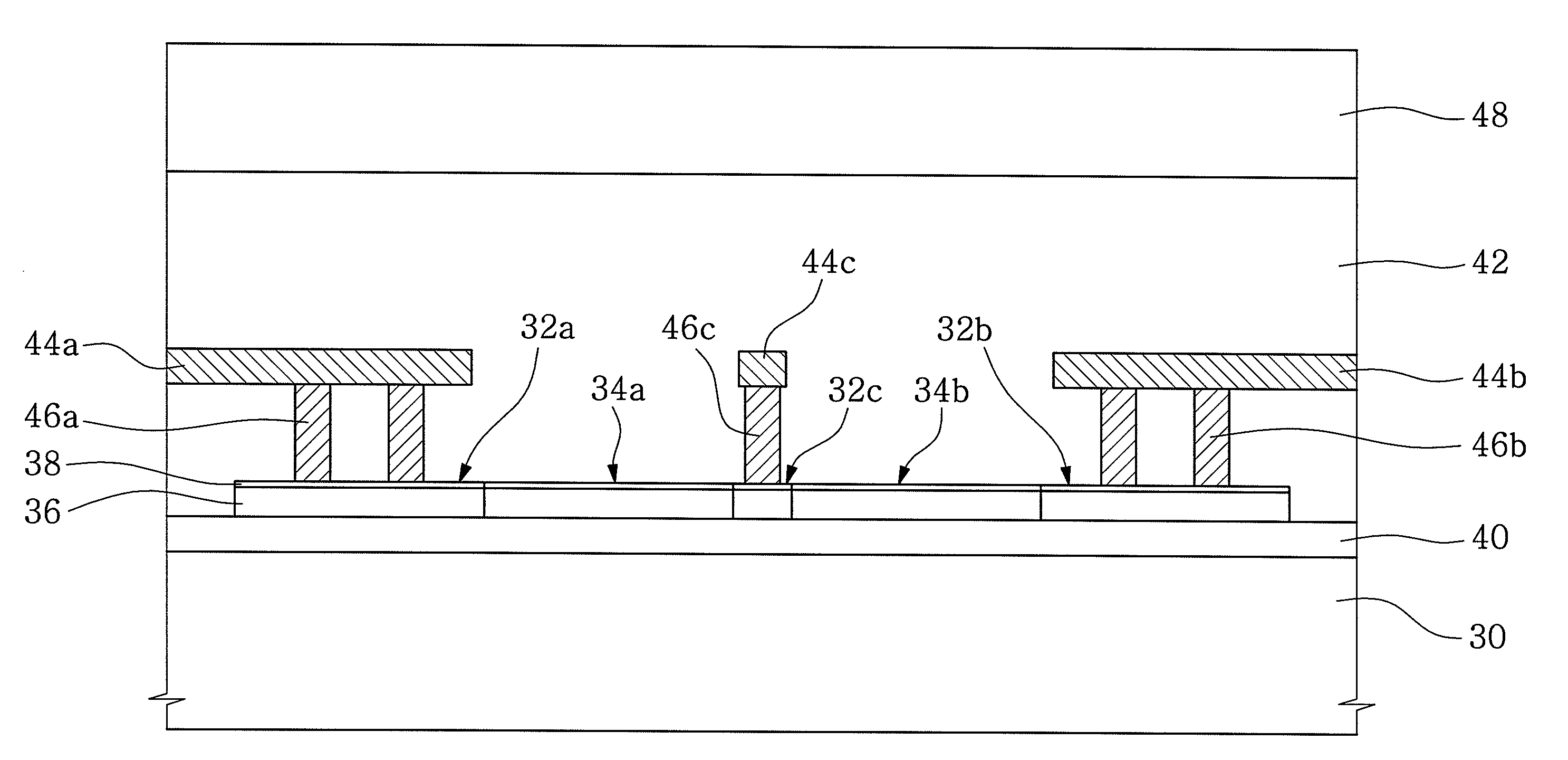
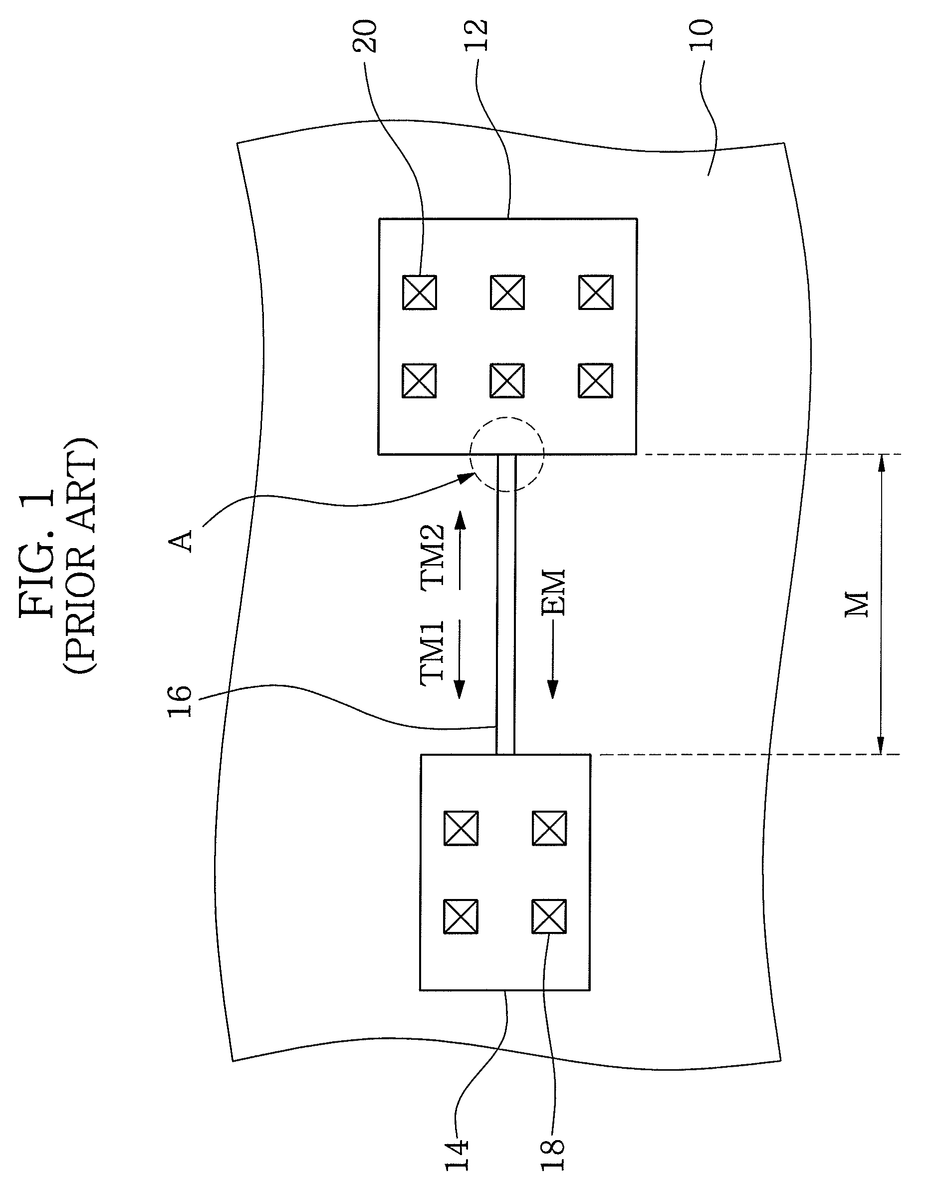
[0038]FIG. 3 is a plan view of an electrical fuse according to an exemplary embodiment of the present invention. FIG. 4 is a cross-sectional view taken along line I-I′ of FIG. 3, which illustrates an electrical fuse a...


PUM


Abstract

Provided are an electrical fuse, a semiconductor device having the same, and a method of programming and reading the electrical fuse. The electrical fuse includes first and second anodes disposed apart from each other. A cathode is interposed between the first and second anodes. A first fuse link couples the first anode to the cathode, and a second fuse link couples the second anode to the cathode.

Description

[0001]This application claims priority to Korean Patent Application No. 10-2006-0134045, filed Dec. 26, 2006, the contents of which are hereby incorporated by reference herein in their entirety.BACKGROUND OF THE INVENTION[0002]1. Technical Field[0003]The present invention relates to an electrical fuse and, more particularly, to an electrical fuse, a semiconductor device having the same, and a method of programming and reading the electrical fuse.[0004]2. Discussion of the Related Art[0005]Semiconductor memory devices (chips) disposed on a semiconductor substrate are electrically tested before an assembly process. As a result, the semiconductor chips are classified as either defective or good. When a malfunction occurs in at least one defective cell of the defective chips, the defective cell is replaced by a redundant cell in a repair process. In order to allow the redundant cell to use an address of the defective cell in write and read modes, predetermined fuses are blown (for examp...

Claims


Application Information

Patent Timeline
Patent Type & Authority Patents(United States)
IPC IPC(8): H01L27/00
CPCG11C17/16G11C17/18H01L23/5256H01L2924/0002H01L2924/00H01L21/82
Inventor NAM, MYUNG-HEEMAEDA, SHIGENOBULEE, JAE-HO
Owner SAMSUNG ELECTRONICS CO LTD
Learn More