Flip chip package structure and carrier thereof

a technology of flip chip and package structure, which is applied in the direction of printed circuit aspects, sustainable manufacturing/processing, final product manufacturing, etc., can solve the problems of poor bonding of gold and tin, circuits coated with solder, and reduce the yield of gold-tin flip chip package structur

Active Publication Date: 2010-09-07
ADVANCED SEMICON ENG INC
View PDF2 Cites 75 Cited by
  • Summary
  • Abstract
  • Description
  • Claims
  • Application Information

AI Technical Summary

Benefits of technology

[0020]The design of the flip chip package structure and the carrier mainly includes a protruding bonding portion of each of the traces of the carrier. The line width of the bonding portion is greater than that of the trace and the bonding portions are arranged along a straight line. The area of the bonding portion is larger and thus, the amount of solder that may be coated thereon is also larger. Thus, in a following reflow process, the solder has a larger cohesive force and bulges as well as consolidates at the same positions to precisely bonding with the bumps. As a result, the problem of poor gold-tin bonding resulted from unfixed places where the solder bulges in the conventional technology may be avoided and the yield of the flip chip package structure may be increased.

Problems solved by technology

However, the circuit has been coated with solder.
However, referring to FIG. 3, if the places where the solder 122 bulges are away from the gold stud bump 130, it often results in a poor bonding of gold and tin and further reduces the yield of the gold-tin flip chip package structure.

Method used


Image

  • Flip chip package structure and carrier thereof
  • Flip chip package structure and carrier thereof
  • Flip chip package structure and carrier thereof

Examples


Embodiment Construction

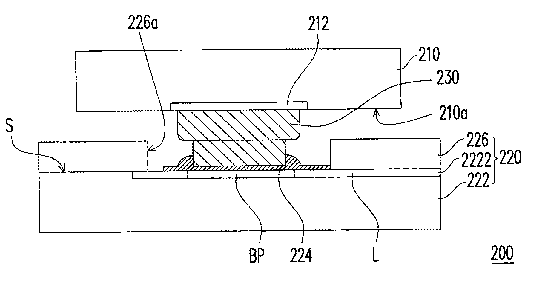
[0031]FIG. 4 is a schematic cross-sectional view of a flip chip package structure according to an embodiment of the present invention. FIG. 5 is a schematic top view of a part of the patterned trace layer of the carrier of the flip chip package structure shown in FIG. 4. First, referring to FIG. 4, a flip chip package structure 200 of the present invention mainly comprises a chip 210, a carrier 220, and a plurality of bumps 230. The components of the flip chip package structure 200 and their relationship will be illustrated in connection with the figures below.

[0032]The chip 210 has a bonding surface 210a and a plurality of bump pads 212 disposed on the bonding surface 210a. The carrier 220 is disposed corresponding to the chip 210 and includes a substrate 222 and a plurality of pre-solders 224. The substrate 222 of the carrier 220 may be a single-layer substrate or a multi-layer substrate. Furthermore, the substrate 222 has a carrying surface S to carry the chip 210 and a patterned...


PUM


Abstract

A flip chip package structure including a chip, a carrier, and a plurality of bumps is provided. The chip has a bonding surface and a plurality of bump pads thereon. The carrier is disposed corresponding to the chip and includes a substrate and a plurality of pre-solders. The substrate has a carrying surface and a patterned trace layer thereon. The patterned trace layer has a plurality of traces, and each of the traces has an outward protruding bonding portion corresponding to the bump. The line width of the bonding portion is greater than that of the trace. The pre-solders are disposed on the bonding portions, respectively. The bumps are disposed between the bump pads and the corresponding pre-solders such that the chip is electrically connected to the carrier through the bumps.

Description

CROSS-REFERENCE TO RELATED APPLICATION[0001]This application claims the priority benefit of Taiwan application serial no. 96139335, filed Oct. 19, 2007. The entirety of the above-mentioned patent application is hereby incorporated by reference herein and made a part of this specification.BACKGROUND OF THE INVENTION[0002]1. Field of the Invention[0003]The present invention relates to a semiconductor package structure and a carrier thereof and more particularly, to a flip chip package structure and a carrier thereof.[0004]2. Description of Related Art[0005]The flip chip (FC) bonding technology is a package technology of bonding a die to a carrier in which a plurality of bumping pads are disposed on an active surface of a die in an area array and bumps are formed on the bumping pads. Then, the die is flipped and the bumping pads on the die surface are electrically and structurally connected to the contacts on the carrier through the bumps. As a result, the die is electrically connected...

Claims


Application Information

Patent Timeline
Patent Type & Authority Patents(United States)
IPC IPC(8): H01L23/48H01L29/40H01L23/52
CPCH01L23/49816H01L23/49838H05K1/111H01L24/16H01L2224/73204H01L2924/01079H05K3/3436H05K3/3452H05K2201/09381H05K2201/09727H05K2201/0989H05K2201/10674H01L24/05H01L24/06H01L24/13H01L2224/05571H01L2224/05573H01L2924/00014Y02P70/50H01L2224/05599
Inventor CHEN, JEN-CHUANSHEN, CHI-CHIHCHANG, HUI-SHANPAN, TOMMY
Owner ADVANCED SEMICON ENG INC
Why Eureka
Try Eureka