Flip chip laser bonding process

a laser bonding and flip chip technology, applied in the direction of metal working equipment, metal working equipment, manufacturing tools, etc., can solve the problems of reducing productivity, inadequate semiconductor packaging method such as a conventional wire bonding method, and thermal compression method having to heat the semiconductor chip for a relatively long time, so as to achieve more uniform distribution

Active Publication Date: 2010-09-28
HANWHA AEROSPACE CO LTD
View PDF16 Cites 7 Cited by
  • Summary
  • Abstract
  • Description
  • Claims
  • Application Information

AI Technical Summary

Problems solved by technology

Accordingly, a semiconductor packaging method such as a conventional wire bonding method is inadequate for newer semiconductor packages, and so new methods have been proposed.
However, the thermal compression method has to heat the semiconductor chip for a relatively long time because heat loss arises in a heat transfer part.
As a result, it takes much time to reach a bonding temperature for the solder bump, and so productivity is reduced and it is impossible to use a material vulnerable to high temperature.
Further, in the thermal compression method, the bonding position may deviate slightly due to the difference in thermal expansion coefficients between the semiconductor chip and the carrier substrate, resulting in a reduction in bonding precision.
Also, the semiconductor chip and the carrier substrate contract after cooling, introducing the risk of a crack or similar damage in the bonded part.
However, in the conventional flip chip bonder, the laser beam for heating the semiconductor chip 80 to the bonding temperature is transferred through the optical fiber 11 without a separate medium and is directly emitted to the semiconductor chip 80, and so the laser beam is not uniformly emitted to the whole region of the semiconductor chip 80.
As a result, energy distribution in the semiconductor chip is very uneven due to the laser beam, which may cause the semiconductor chip 80 to be damaged, bonding quality to be deteriorated, or similar problems.
Therefore, in the flip chip bonding, if the intensity and the amount of the laser beam are reduced with respect to the energy in the center region, there is an energy shortage in the surrounding region, thereby causing deterioration in the bonding quality.
On the other hand, if the intensity and the amount of the laser beam are increased with respect to the energy in the surrounding region, excessive energy is applied to the center region, thereby causing the semiconductor chip 80 to be damaged or the like.

Method used


Image

  • Flip chip laser bonding process
  • Flip chip laser bonding process
  • Flip chip laser bonding process

Examples


Embodiment Construction

[0054]Embodiments of the present invention will be described below in more detail with reference to the accompanying drawings. The present invention may, however, be embodied in different forms and should not be construed as being limited to the embodiments set forth herein. Rather, these embodiments are provided to assist one skilled in the art to understand the invention. Like reference numerals refer to like elements throughout the accompanying figures.

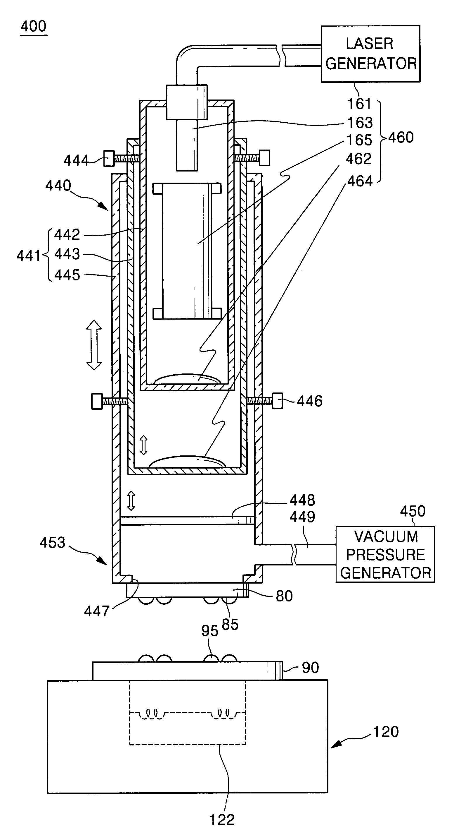
[0055]Referring to FIG. 5, a flip chip bonder 100 according to a first exemplary embodiment of the present invention includes: a bonding stage 120 on which a substrate 90 formed with a solder bump 95 is placed; a bonding head 140 which is disposed above the bonding stage 120, picks up a semiconductor chip 80 formed with a solder bump 85 from a flip head (not shown) or the like, and bonds the solder bump 85 of the picked-up semiconductor chip 80 to the solder bump 95 of the substrate 90; a chip heating apparatus 160 to heat the semi...


PUM

PropertyMeasurementUnit
wavelengthaaaaaaaaaa
bonding temperatureaaaaaaaaaa
outer circumferenceaaaaaaaaaa

Abstract

An apparatus for heating a chip includes: a laser generator for emitting a laser beam to a semiconductor chip to heat the semiconductor chip; and a beam intensity adjuster disposed on a laser emission path between the semiconductor chip and the laser generator to equalize the intensity of the laser beam to be emitted to the semiconductor chip. A flip chip bonder having the chip heating apparatus, and a method for bonding a flip chip using the same are also provided.

Description

CROSS-REFERENCE TO RELATED APPLICATION[0001]This application claims the benefit of Korean Patent Application No. 2007-0039741, filed Apr. 24, 2007, the disclosure of which is hereby incorporated herein by reference in its entirety.BACKGROUND OF THE INVENTION[0002]1. Field of the Invention[0003]The present invention relates to an apparatus and method for bonding a semiconductor chip on a substrate, and more particularly, to an apparatus for heating a semiconductor chip using a laser beam, a flip chip bonder having the apparatus, and a method for bonding a flip chip using the same.[0004]2. Description of the Related Art[0005]In recent times, electronic devices have become smaller in size but also have increased functionality, and accordingly tend to include a highly integrated and high performance semiconductor chip.[0006]Likewise, to follow this trend, a semiconductor package that protects such a semiconductor chip from various exterior environmental factors, e.g., dust or moisture, ...

Claims


Application Information

Patent Timeline
Patent Type & Authority Patents(United States)
IPC IPC(8): H01L21/44
CPCB23K1/0056B23K26/0626H01L24/81H01L24/75B23K2201/40H01L2224/75251H01L2224/75743H01L2224/81121H01L2224/81193H01L2224/81203H01L2224/81224H01L2224/81801H01L2924/01033H01L2924/01082H01L2924/014B23K2101/40H01L21/268
Inventor KIM, SUNG-WOOK
Owner HANWHA AEROSPACE CO LTD
Why Eureka
Try Eureka