Programmable logic block having reduced output delay during RAM write processes when programmed to function in RAM mode

Active Publication Date: 2010-09-28
XILINX INC
View PDF80 Cites 61 Cited by
  • Summary
  • Abstract
  • Description
  • Claims
  • Application Information

AI Technical Summary

Benefits of technology

[0012]The invention provides a programmable logic block that provides an improved output delay by bypassing the memory array and multiplexer structure when programmed to function as a random access memory (RAM) and a new value is written to the RAM. According to one embodiment, a programmable logic block includes memory cells, a multiplexer structure, a memory element, a bypass select multiplexer, and a control circuit. The memory cells implement a RAM driven by a write data input signal and a write en

Problems solved by technology

Further, a PLD interconnect structur

Method used


Image

  • Programmable logic block having reduced output delay during RAM write processes when programmed to function in RAM mode
  • Programmable logic block having reduced output delay during RAM write processes when programmed to function in RAM mode
  • Programmable logic block having reduced output delay during RAM write processes when programmed to function in RAM mode

Examples


Embodiment Construction

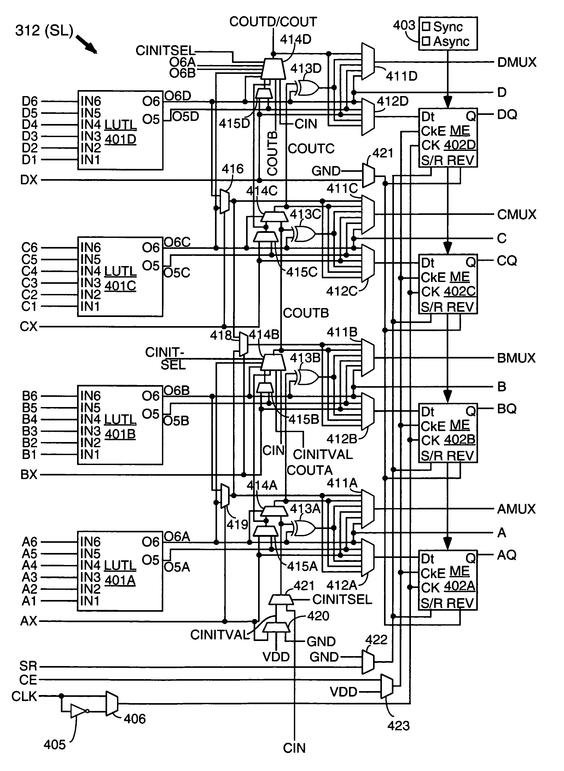
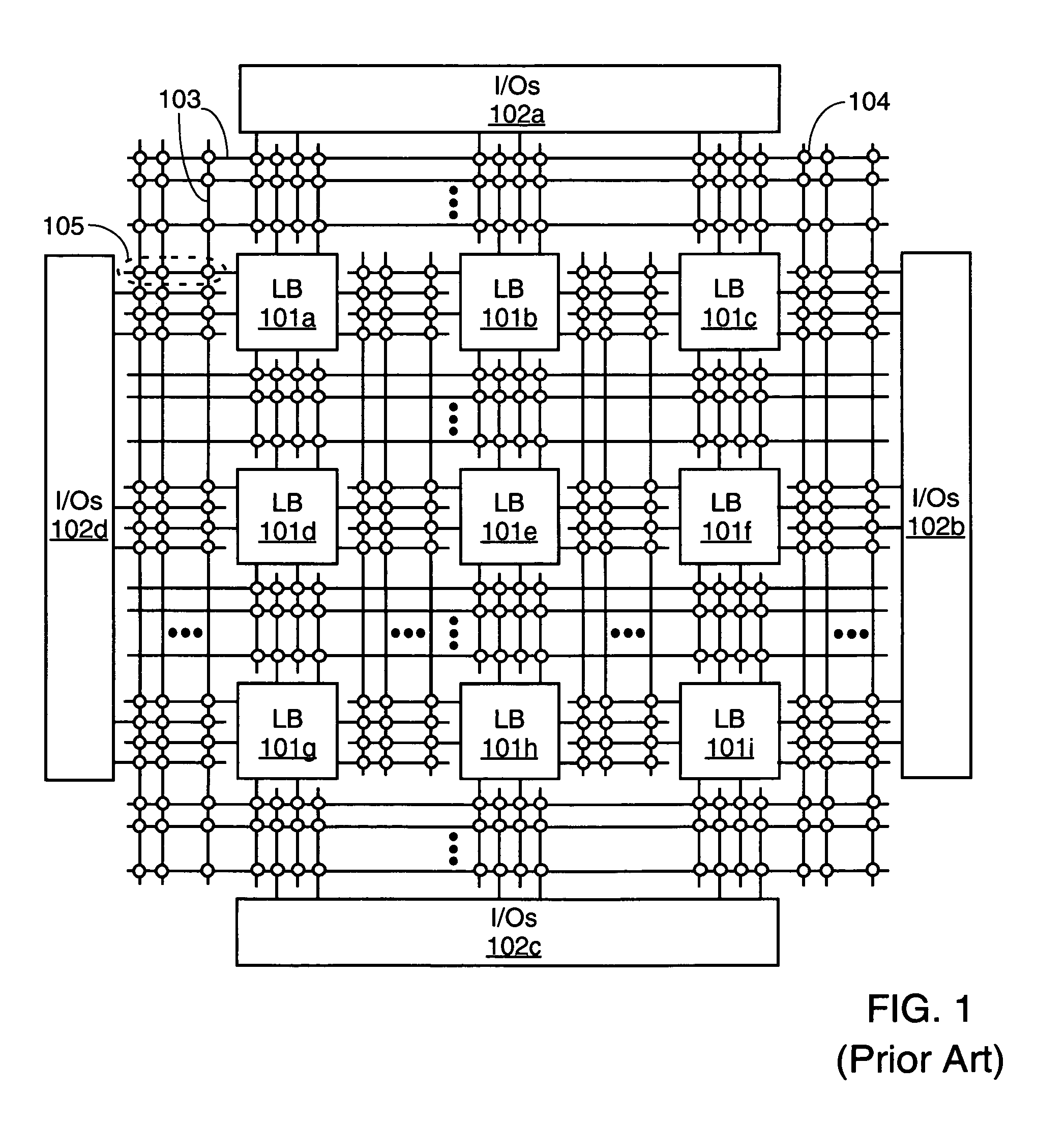
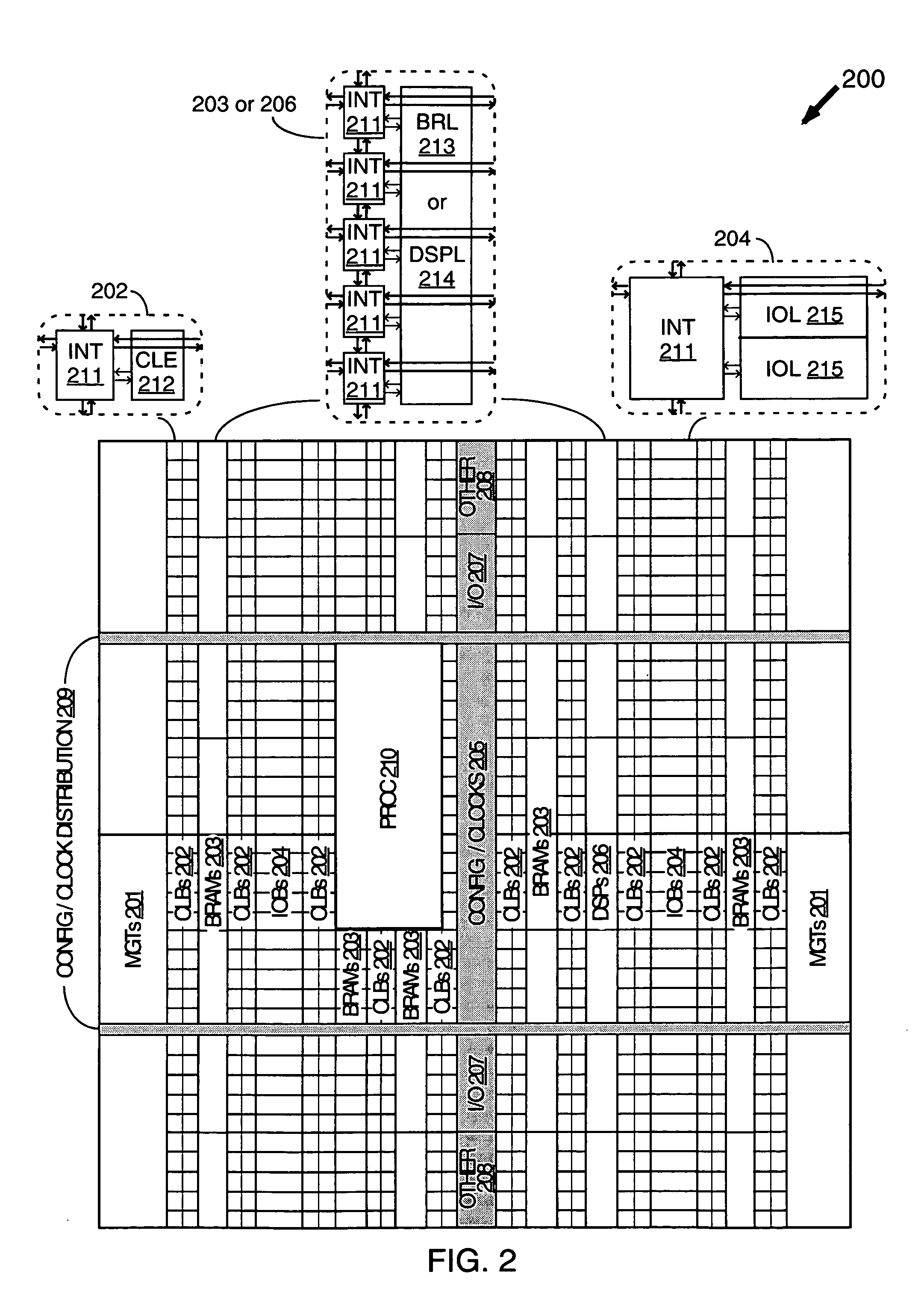
Legend 1 (Applied Throughout): Interconnect Signal Naming ConventionsL_nSignal “n” in slice LM_nSignal “n” in slice Mxy5B#“Pent” interconnect line, “Beginning” or entering point.If “y” is North, South, East, or West, denotes 1 of 3 “diagonal” interconnect linesextending 3 tiles in “x” direction then turning in “y” direction for 2 tiles. If “y” is Lor R, denotes 1 of 3 “straight” interconnect lines extending 5 tiles in “x” direction.xy5M#“Pent” interconnect line, “Middle” exiting point at turning tilexy5E#“Pent” interconnect line, “End” exiting pointxy2B#“Double” interconnect line, “Beginning” or entering point.If “y” is North, South, East, or West, denotes 1 of 3 “diagonal” interconnect linesextending 1 tile in “x” direction then turning in “y” direction for 1 tile. If “y” is Lor R, denotes 1 of 3 “straight” interconnect lines extending 2 tiles in “x” direction.xy2M#“Double” interconnect line, “Middle” exiting point at turning tilexy2E#“Double” interconnect line, “End” exiting point...


PUM


Abstract

A programmable logic block provides an improved output delay by bypassing the memory array and multiplexer structure when programmed to function as a random access memory (RAM) and a new value is written to the RAM. A programmable logic block includes memory cells, a multiplexer structure, a memory element, a bypass select multiplexer, and a control circuit. The memory cells implement a RAM driven by a write data input signal and a write enable signal. Each memory cell drives an input terminal of the multiplexer structure. Under the control of the write enable signal, a bypass select multiplexer selects either the write data input signal (in RAM mode) or the output terminal of the multiplexer structure (in another mode), and passes the selected signal to a memory element. Thus, when in RAM mode, write data is simultaneously written to a specified location in the RAM and to the memory element.

Description

FIELD OF THE INVENTION[0001]The invention relates to programmable integrated circuits (ICs). More particularly, the invention relates to a programmable logic block that provides an improved output delay by bypassing the memory array and multiplexer structure when programmed to function as a random access memory (RAM) and a new value is written to the RAM.BACKGROUND OF THE INVENTION[0002]Programmable logic devices (PLDs) are a well-known type of integrated circuit that can be programmed to perform specified logic functions. One type of PLD, the field programmable gate array (FPGA), typically includes an array of programmable tiles. These programmable tiles can include, for example, input / output blocks (IOBs), configurable logic blocks (CLBs), dedicated random access memory blocks (BRAM), multipliers, digital signal processing blocks (DSPs), processors, clock managers, delay lock loops (DLLs), and so forth.[0003]Each programmable tile typically includes both programmable interconnect ...

Claims


Application Information

Patent Timeline
IPC IPC(8): G11C7/00
CPCH03K19/17728H03K19/17736H03K19/1776
Inventor CHIRANIA, MANOJKONDAPALLI, VENU M.
Owner XILINX INC
Why Eureka
Try Eureka