Display device and driving method thereof

a technology of a display device and a driving method, which is applied in the direction of static indicating devices, instruments, electroluminescent light sources, etc., can solve the problem of insufficient correction of fluctuations in the current value of the driving transistor due to the variation in mobility, and achieve the effect of canceled fluctuations

Inactive Publication Date: 2010-10-05
SEMICON ENERGY LAB CO LTD
View PDF140 Cites 61 Cited by
  • Summary
  • Abstract
  • Description
  • Claims
  • Application Information

AI Technical Summary

Benefits of technology

[0011]In view of the above-mentioned problems, an object of the present invention is to prevent luminance from being influenced by not only a variation in a current value due to a threshold voltage but also a variation in the current value due to mobility.
[0015]In the present invention, with the above-described structure, the value of a voltage for correction which functions as a correction term is changed in accordance with a potential of a video signal. That is, when a high level of grayscale is displayed, an initial potential for correction which makes the absolute value of the voltage for correction large is applied to a pixel; and when a low level of grayscale is displayed, the initial potential for correction which makes the absolute value of the voltage for correction small is applied to the pixel. In this manner, when a value of the voltage for correction is changed in accordance with the potential of the video signal, correction can be performed so as to make a current Id closer to 0 even when the level of grayscale is lowered, that is, even when a difference between the potential of the video signal and a reference potential is small. Therefore, not only in the case where a high level of grayscale is displayed but also in the case where a low level of grayscale is displayed, a fluctuation in a current value of a driving transistor due to a variation in mobility can be suppressed, so that a variation in luminance due to the fluctuation can be suppressed.
[0016]Therefore, the present invention can adequately prevent not only a variation in a current value due to the threshold voltage but also a variation in a current value due to mobility from influencing luminance, with respect to all the levels of grayscale to be displayed.

Problems solved by technology

That is, in the driving method described above, the fluctuation in the current value of the driving transistor due to the variation in the mobility is not corrected adequately to be canceled.

Method used


Image

  • Display device and driving method thereof
  • Display device and driving method thereof
  • Display device and driving method thereof

Examples


embodiment mode 1

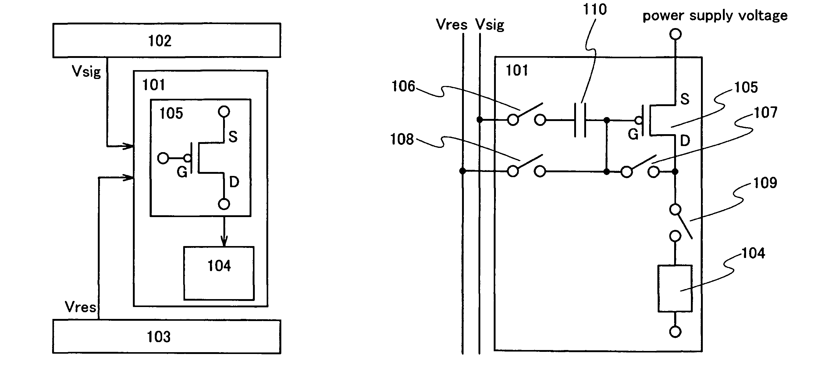
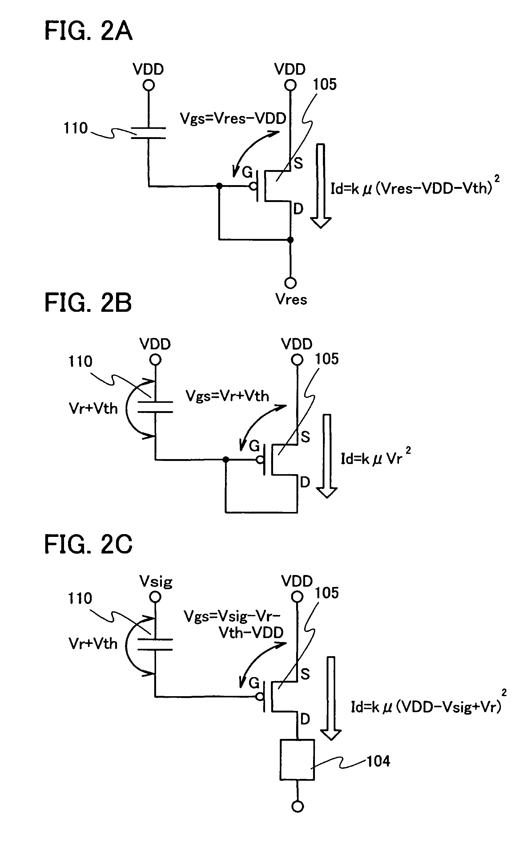
[0036]FIG. 1A is a block diagram of a display device of the present invention. The display device of the present invention includes a pixel 101, a signal line driver circuit 102 which applies a potential Vsig of a video signal to the pixel 101, and a reset line driver circuit 103 which applies an initial potential Vres for correction to the pixel 101 before the potential Vsig of the video signal is applied to the pixel 101. The pixel 101 includes at least a light-emitting element 104 which displays grayscale in accordance with a value of a current supplied and a driving transistor 105 which controls the value of the current supplied to the light-emitting element 104.

[0037]The initial potential Vres for correction applied to the pixel 101 is applied to a gate (G) and a drain (D) of the driving transistor 105. In addition, a potential which is obtained by subtracting a voltage for correction obtained by the initial potential Vres for correction from the potential Vsig of the video sig...

embodiment mode 2

[0068]In this embodiment mode, a specific structure and operation of a pixel included in a display device of the present invention will be described.

[0069]FIG. 5A shows a circuit diagram of a pixel in this embodiment mode. A pixel 200 shown in FIG. 5A includes, in addition to a light-emitting element 201 and a driving transistor 202, a switching transistor 203 which samples a video signal having the potential Vsig, a transistor 204 which controls connection between a gate (G) and a drain (D) of the driving transistor 202, a transistor 205 which controls application of the initial potential Vres for correction to the gate (G) of the driving transistor 202, a transistor 206 which selects whether the drain of the driving transistor 202 is set to be in a floating state or not, a capacitor 207 for holding a voltage between the gate and a source of the driving transistor 202 during the correction period, and a capacitor 208 for holding a potential difference between the potential of the v...

embodiment mode 3

[0084]In this embodiment mode, a more specific structure and operation of a pixel included in a display device of the present invention will be described.

[0085]FIG. 6A shows a circuit diagram of a pixel in this embodiment mode. A pixel 300 shown in FIG. 6A includes, in addition to a light-emitting element 301 and a driving transistor 302, a switching transistor 303 which samples a video signal having the potential Vsig, a transistor 304 which controls connection between a gate (G) and a drain (D) of the driving transistor 302, a transistor 305 which controls application of the initial potential Vres for correction to the gate (G) of the driving transistor 302, a transistor 306 which selects whether the drain of the driving transistor 302 is set to be in a floating state or not, a capacitor 307 which holds a voltage between the gate and the source of the driving transistor 302 during the correction period, a capacitor 308 which holds a potential difference between the potential of th...


PUM


Abstract

A display device in which not only a variation in a current value due to a threshold voltage but also a variation in a current value due to mobility are prevented from influencing luminance with respect to all the levels of grayscale to be displayed. After applying an initial potential for correction to a gate and a drain of a driving transistor, the gate and the drain of the driving transistor is kept connected in a floating state, and a voltage is held in a capacitor before a voltage between the gate and a source of the driving transistor becomes equal to a threshold voltage. When a voltage obtained by subtracting the voltage held in the capacitor from a voltage of a video signal is applied to the gate and the source of the driving transistor, a current is supplied to a light-emitting element. A value of an initial voltage for correction differs in accordance with the voltage of the video signal.

Description

BACKGROUND OF THE INVENTION[0001]1. Field of the Invention[0002]The present invention relates to a display device in which a transistor is provided for each pixel and a driving method thereof.[0003]2. Description of the Related Art[0004]Since display devices using light-emitting elements have high visibility, are suitable for reduction in thickness, and do not have limitations on viewing angles, they have attracted attention as display devices which can take the place of CRTs (cathode ray tubes) or liquid crystal display devices. Specifically proposed structures of active matrix display devices using light-emitting elements are different depending on manufacturers. However, in general, at least a light emitting element, a transistor (a switching transistor) which controls input of video signals to pixels, and a transistor (a driving transistor) which controls value of current supplied to the light-emitting elements are provided for each pixel.[0005]On the other hand, thin film trans...

Claims


Application Information

Patent Timeline
Patent Type & Authority Patents(United States)
IPC IPC(8): H01L31/14G09G3/20G09G3/30H01L51/50H05B44/00
CPCG09G3/325H01L27/1255H01L27/1266G09G2300/0439G09G2300/0819G09G2300/0852G09G2310/0262G09G2310/027G09G2300/0866H01L2924/13069
Inventor MIYAKE, HIROYUKI
Owner SEMICON ENERGY LAB CO LTD
Why Eureka
Try Eureka