Asymmetrical flat antenna, method of manufacturing the asymmetrical flat antenna, and signal-processing unit using the same

a technology of asymmetrical flat antenna and flat antenna, which is applied in the direction of waveguide type devices, substantially flat resonant elements, and resonant antennas, etc., can solve the problem of difficult to keep any desired antenna characteristics that have been designed in a mutual relationship between the antenna and the metal, and achieves convenient connection, improved reflection characteristics, and efficient near-distance wireless communication processing

Inactive Publication Date: 2010-10-26
SONY CORP
View PDF9 Cites 4 Cited by
  • Summary
  • Abstract
  • Description
  • Claims
  • Application Information

AI Technical Summary

Benefits of technology

[0014]In the flat patch antenna as disclosed in Japanese Patent Application Publication No. 2005-192183, a matching circuit is often disposed between the antenna pattern and the power line, thereby preventing power from being supplied from the pins of the LSI directly to the antenna.
[0016]Further, if any metal approaches a board or LSI device loaded with the antenna, the characteristics may be deteriorated thereby. This causes a unidirectional antenna to be used therefor. In case of performing broadband wireless communication processing using a broadband communication chip as described in Japanese Patent Application Publication No. 2004-220264, radio wave which turns to communication noise can be absorbed to some extent by a radio wave absorption body. If, however, the working frequency of an electronic device rises so that an amount of information handled by wireless communication can be increased, such the information may be transmitted at real time in a short time if considering continuity of, for example, transmitted images.
[0018]Accordingly, it is desirable to provide an asymmetrical flat antenna in which the band of its flat antenna can be expanded as compared with the band of a rectangular patch antenna with reference to its ratio of bandwidth while the frequency resonance point in antenna reflection characteristic can be improved by devising the configuration of the flat antenna, a method of manufacturing the asymmetrical flat antenna, and a signal-processing unit using the asymmetrical flat antenna.
[0021]This asymmetrical configuration enables the frequency resonance point in the reflection characteristic of antenna to be changed, thereby allowing the band of the asymmetrical flat antenna as the embodiment of the present invention to be expanded as compared with the band of the rectangular patch antenna with respect to its ratio of bandwidth. The asymmetrical flat antenna as the embodiment of the present invention can be connected with the LSI device on a board on which the LSI device is mounted or within the LSI device and can have broadband performance whose ratio of bandwidth is 11% or more and some extend of directivity in which the asymmetrical flat antenna as the embodiment of the present invention operates under a condition other than far field with a matching circuit possessed in the antenna pattern. Such the antenna characteristic enables the lamination structure and the antenna pattern of the antenna to exert effects on multipath. This allows freedom of antenna arrangement in an electronic device to be secured and any cost accompanying wiring to be reduced.
[0025]In the embodiment of the signal-processing unit according to the present invention, the asymmetrical flat antenna is used when the asymmetrical flat antenna is connected in the signal-processing unit in order to perform any signal processing. Accordingly, the reflection characteristic thereof can be improved as compared by that of the signal-processing unit including the rectangular patch antenna. This enables the most efficient near distance wireless communication processing using the asymmetrical flat antenna that is operable under a condition other than the far field to be performed. That is, by the embodiment of the signal-processing unit according to the present invention, it is possible to maintain easy connection with the LSI device on a board on which an available LIS device is mounted or within the LSI device during wireless communication within a casing and to have a broadband antenna whose a ratio of bandwidth is 11% or more. Such the broadband antenna has a matching circuit near its antenna pattern and can execute wireless communication processing with a signal-processing board within a electronic device using the broadband antenna. It is also possible to preclude a step of wiring a signal line between the LSI boards and attain a high speed transmission of information between the LSI boards.

Problems solved by technology

Thus, if such the rectangular patch antenna 10 is used under the above condition, it is difficult to keep any desired antenna characteristics that have been designed in a mutual relationship between the antenna and the metal.

Method used


Image

  • Asymmetrical flat antenna, method of manufacturing the asymmetrical flat antenna, and signal-processing unit using the same
  • Asymmetrical flat antenna, method of manufacturing the asymmetrical flat antenna, and signal-processing unit using the same
  • Asymmetrical flat antenna, method of manufacturing the asymmetrical flat antenna, and signal-processing unit using the same

Examples


third embodiment

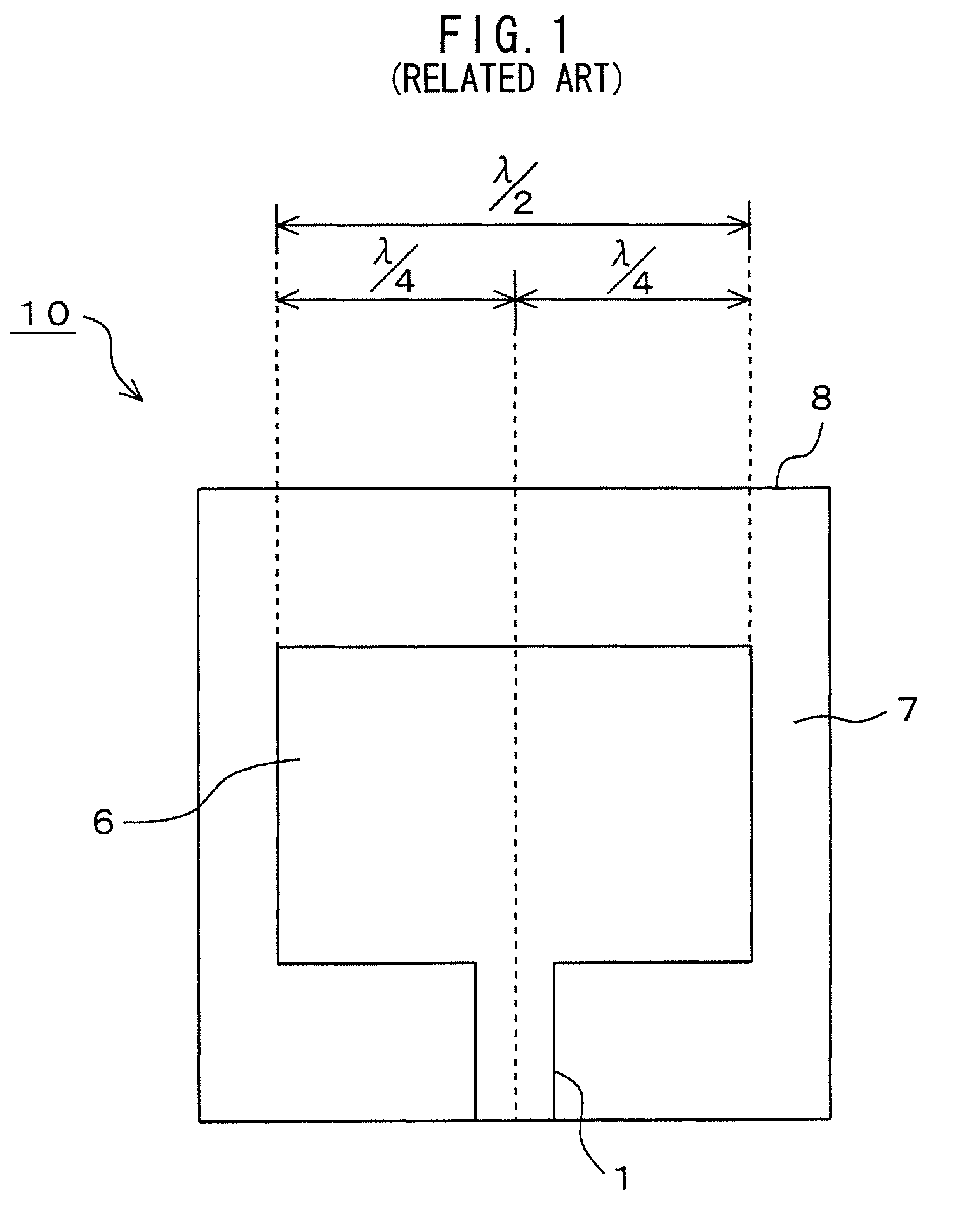
[0080]FIG. 5 shows a configuration of an asymmetrical flat antenna 110 as the invention, which is compared with the rectangular patch antenna 10. The asymmetrical flat antenna 100 of embodiments of the present invention is also compared with the rectangular patch antenna 10. Thus, the asymmetrical flat antenna 110 is indirectly compared with the asymmetrical flat antenna 100. The asymmetrical flat antenna 110 shown in FIG. 5 is manufactured by adding components which change the resonance frequency to the rectangular patch antenna 10 shown in FIG. 1.

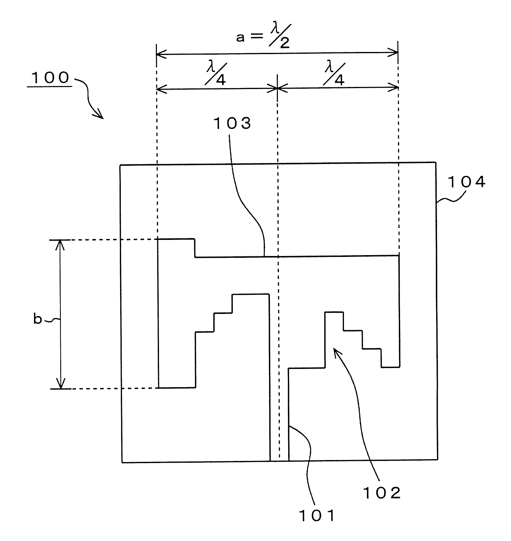
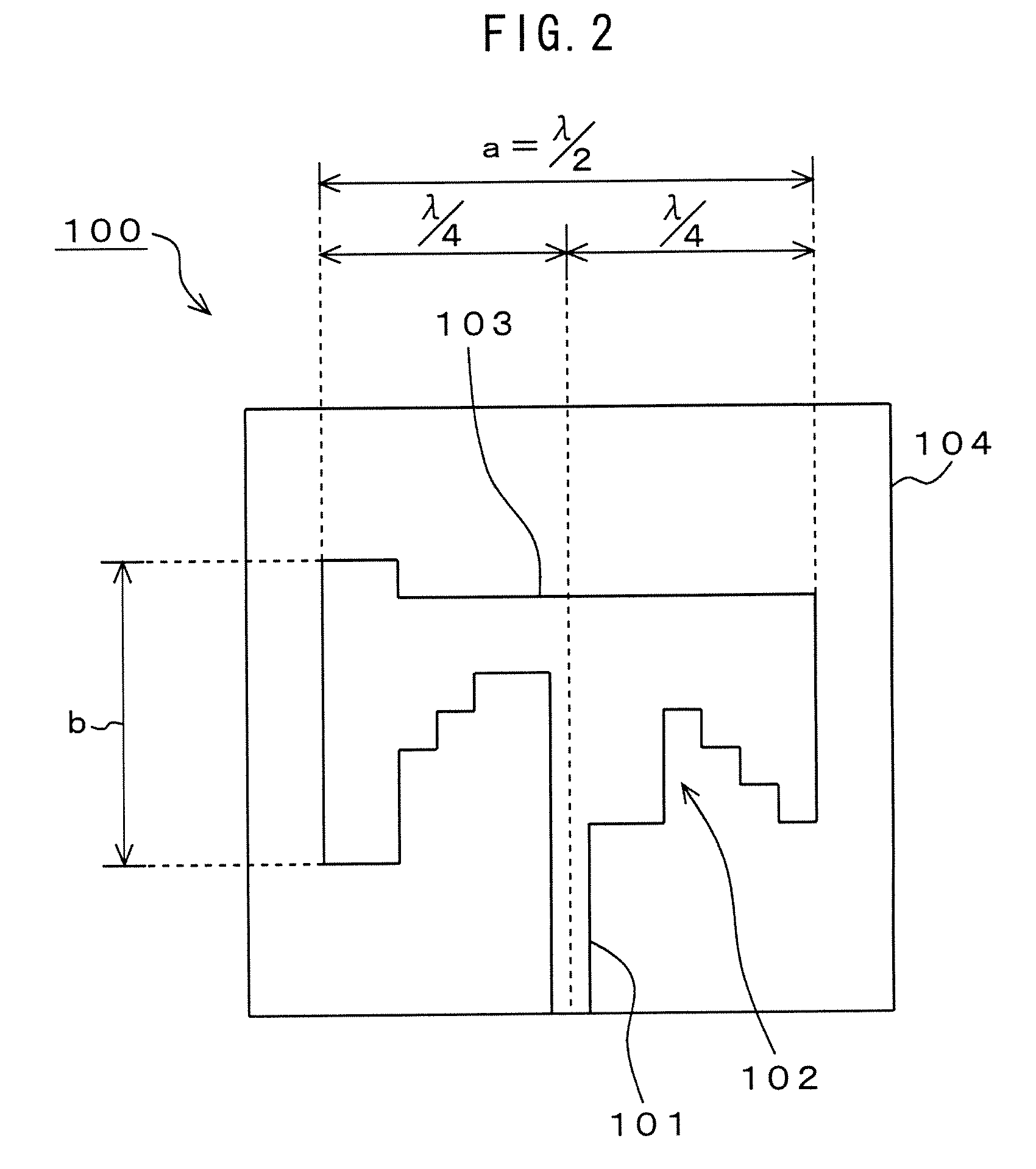
[0081]An antenna pattern 103A has a length of λ / 2 in the longitudinal direction where λ is the wavelength of working frequency. When the antenna pattern 103A is divided into two parts, namely, λ / 4 each on the right and left sides thereof with respect to a center of the conductive power supply pattern 101, the shape of the right part thereof is different from that of the left part thereof. A projection to the right direction from the right...

first embodiment

[0091]In the FIG. 7, resonance frequencies of the rectangular patch antenna 10 indicate 4.5 GHz and 5.3 GHz. Resonance frequencies of the asymmetrical flat antenna 100 as the present invention indicate 3.8 GHz and 5.8 GHz. According to the reflection characteristic III of the asymmetrical flat antenna 100, the upper limit frequency fh and the lower limit frequency fl are 6.0 [GHz] and 3.6 [GHz], respectively, when its characteristic curve passes S11=−5.00 E+00 and thus, the band C (=bandwidth fb) is 2.4 [GHz].

[0092]As indicated with arrows shown in FIG. 7, the band C can be improved as compared with the band A. This example indicates that the band C is expanded to 2.4 times more than the band B shown in FIG. 6 and is expanded to 5.3 times more than the band A shown therein. Thus, the asymmetrical flat antenna 100 as the first embodiment of the present invention can expand the bandwidth fb of the band C as compared with the bands A, B of the rectangular patch antenna 10 as related ar...

fourth embodiment

[0123]FIG. 15 shows a configuration of a signal-processing unit 200 as the invention to which the asymmetrical flat antenna 100 is applied. In this embodiment, the antenna pattern 103 is laid out (disposed) on a lamination structured device in which an ordinary multilayered board or dielectric is sandwiched between metal layers so as to form an antenna 111. This antenna 111 is connected to an LSI device 112 for signal processing through a transmission path 115. That is, in this structure, the dielectric is sandwiched between the antenna pattern 103 and the GND layer 213.

[0124]In the signal-processing unit 200 shown in FIG. 15, the signal-processing board is constituted to have the antenna 111 and the LSI device 112 on the multilayered board 214. The antenna 111 and the LSI device 112 are connected via the transmission path 115 so as to perform any signal processing. As the LSI device 112, one having a wireless IC (semiconductor integrated circuit) internally is used.

[0125]As the ant...


PUM


Abstract

An asymmetrical flat antenna contains an insulation layer. The antenna also contains a conductive power supply pattern that is provided on the insulation layer and a conductive antenna pattern that extends from the power supply pattern and is provided on the insulation layer. The conductive antenna pattern has an asymmetrical configuration with respect to the power supply pattern.

Description

CROSS-REFERENCE TO RELATED APPLICATION[0001]The present invention contains subject matter related to Japanese Patent Application JP 2006-053732 filed in the Japanese Patent Office on Feb. 28, 2006, the entire contents of which being incorporated herein by reference.BACKGROUND OF THE INVENTION[0002]1. Field of the Invention[0003]The present invention relates to an asymmetrical flat antenna, a method of manufacturing the asymmetrical flat antenna, and a signal-processing unit using this antenna.[0004]2. Description of Related Art[0005]An antenna has been often designed and developed so that it is suitably used in an electronic device having portability, a communication device that is used in a home where it is difficult to wire a communication cable therein or is used for a long distance in a precinct or a building, and the like. That is, the development and design of the antenna have been often carried out aiming at how efficiently to emit radio wave to a long distance and for its ba...

Claims


Application Information

Patent Timeline
Patent Type & Authority Patents(United States)
IPC IPC(8): H01Q1/50H01Q1/38H01P11/00H01Q13/08H01Q23/00
CPCH01Q1/38H01Q9/0407H01Q9/285H01Q1/242
Inventor YOSHIOKA, MASAHIRONAKANISHI, TAKASHIWADA, SEIJIKONDO, TETSUJIRO
Owner SONY CORP
Why Eureka
Try Eureka