
Delay-locked loop circuits and method for generating transmission core clock signals

a delay-locked loop and clock signal technology, applied in the field of semiconductor memory devices, can solve the problems of dll circuits according to a conventional approach having an error occurrence possibility, dcc circuits having a limitation in correcting a dll circuits having a limitation in the duty cycle of input clock signals, etc., to achieve the effect of reducing error occurrence and easy control

Inactive Publication Date: 2010-11-02
SAMSUNG ELECTRONICS CO LTD
View PDF13 Cites 15 Cited by
  • Summary
  • Abstract
  • Description
  • Claims
  • Application Information

AI Technical Summary

Benefits of technology

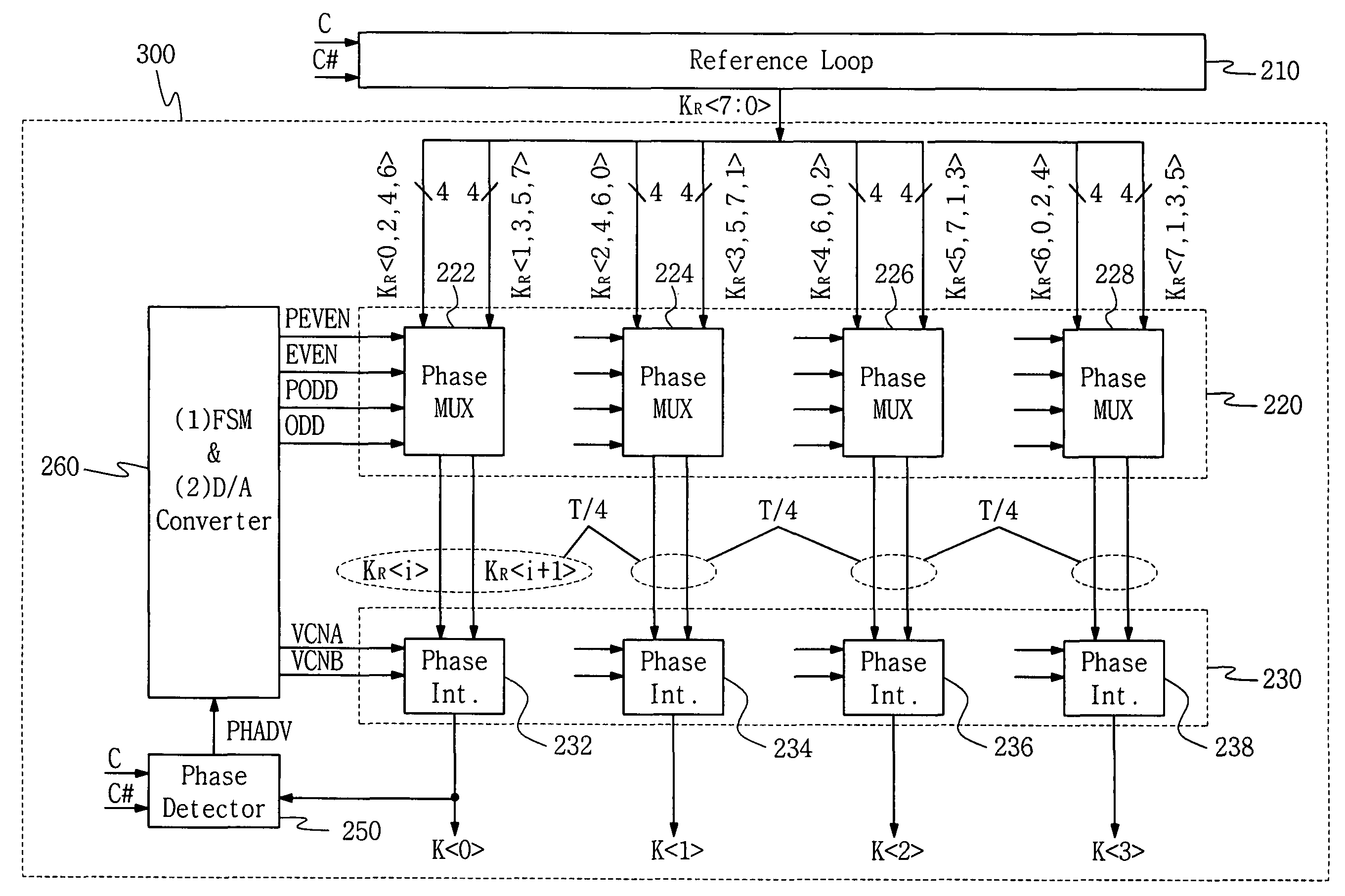
The present disclosure provides a delay locked loop (DLL) circuit and method for generating transmission core clock signals. The circuit and method do not require a DCC circuit, which reduces phase error of transmission core clock signals. The circuit includes a delay circuit unit that delays the external clock signal through a chain of delay units and generates a plurality of reference clock signals with different phases. The transmission core clock signals are generated by independently selecting and controlling two reference clock signals from the reference clock signals. The circuit and method can be easily controlled and can generate transmission core clock signals with low phase error.

Problems solved by technology

The phase locked loop circuit is sensitive to jitter of the input clock signal, is greatly affected by internal noise, and is unstable as compared with the delay-locked loop circuit.
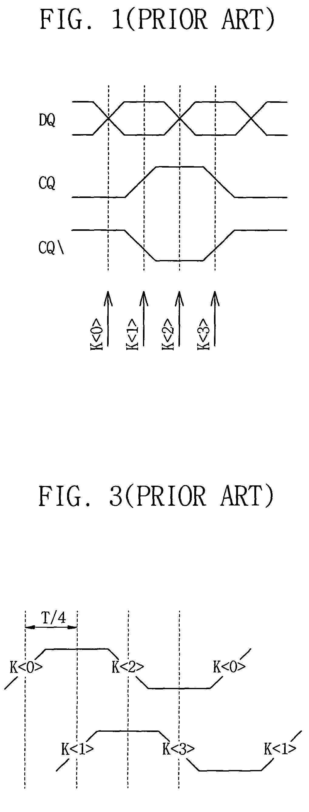
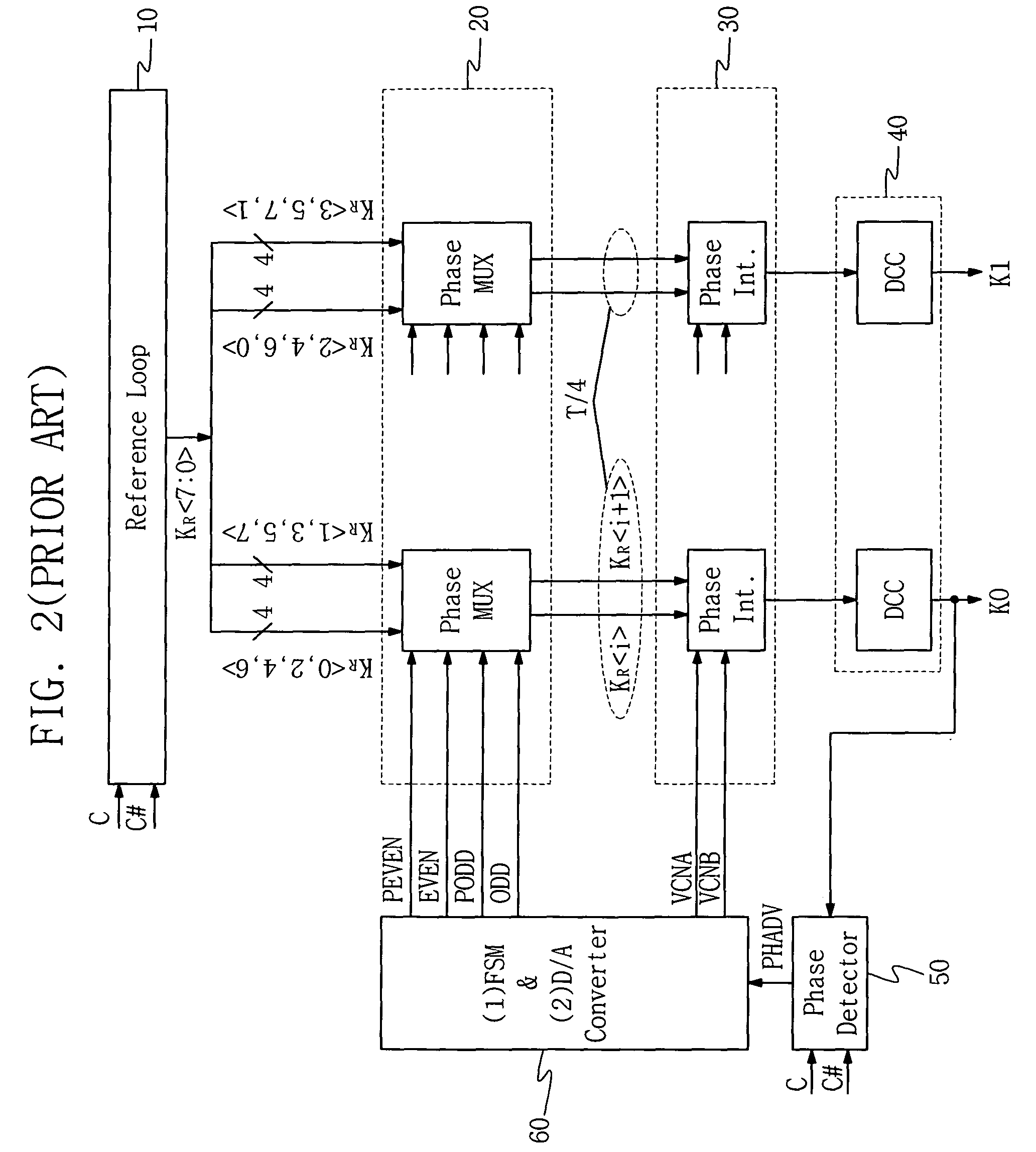
Such DLL circuits according to a conventional approach have an error occurrence possibility because of the use of rising edges and falling edges of the first internal clock signal K0 and the second internal clock signal K1 provided as transmission core clock signals.
Thus, a clock buffer is additionally needed in the DLL circuit and / or on an end of clock tree, and errors may be caused.
Furthermore, a DCC circuit has a limitation in correcting a duty cycle of an input clock signal, and it is difficult to generate four transmission core clock signals having a precise phase difference due to errors of the DCC circuit itself, etc.
In addition, in cases such as the DLL circuit shown in FIG. 4, error occurrence may become high when a delay control is not precise in the delay unit.

Method used


Image

  • Delay-locked loop circuits and method for generating transmission core clock signals
  • Delay-locked loop circuits and method for generating transmission core clock signals
  • Delay-locked loop circuits and method for generating transmission core clock signals

Examples


Embodiment Construction

[0050]The present disclosure provides a delay-locked loop (DLL) circuit and a method for generating all transmission core clock signals used in a semiconductor memory device without employing a duty cycle correction (DCC) circuit. Hereinafter, exemplary embodiments of the present disclosure will be described in detail with reference to FIGS. 6 to 10. It will be understood by those of ordinary skill in the pertinent art that the present invention can be embodied in numerous different forms and is not limited to the following described embodiments. The following embodiments are exemplary in nature.

[0051]FIG. 6 is a block diagram of a delay-locked loop (DLL) circuit according to an exemplary embodiment of the disclosure. Referring to FIG. 6, a DLL circuit includes a delay circuit unit 210 and a transmission core clock signal generating unit 300. The delay circuit unit 210 delays an external clock signal C,C# applied through a plurality of delay units configured in a chain type, and out...


PUM


Abstract

A delay-locked loop (DLL) circuit and a method for generating transmission core clock signals are provided, where the DLL circuit receives an applied external clock signal and generates a transmission core clock signal, the DLL circuit includes a delay circuit unit and a transmission core clock signal generating unit, the delay circuit unit delays the external clock signal through a plurality of delay units configured in a chain type and outputs a plurality of reference clock signals having different phases, the transmission core clock signal generating unit independently selects and controls two reference signals from the plurality of reference clock signals and thus independently generates transmission core clock signals by the number corresponding to ½ times the number of reference clock signals, and the transmission core clock signals have different phases and a period equal to a period of the external clock signal, wherein transmission core clock signals having a precise phase difference are generated individually and independently.

Description

CROSS-REFERENCE TO RELATED APPLICATION[0001]This application claims foreign priority under 35 U.S.C. §119 to Korean Patent Application No. 10-2005-0034348, filed on Apr. 26, 2005, in the Korean Intellectual Property Office, which is herein incorporated by reference in its entirety.BACKGROUND[0002]The present disclosure relates to semiconductor memory devices. More particularly, the present disclosure relates to-a delay-locked loop (DLL) circuits for generating transmission core clock signals used in semiconductor memory devices.[0003]Rapid development in semiconductor technology has brought about successful developments for digital systems such as personal computers, Portable Digital Assistants (PDA) or portable communication systems. However, an operating speed of peripheral devices could not overtake an operating speed of microprocessors in spite of an improved transmission rate of data and an improved operating speed of peripheral devices such as memories and communication device...

Claims


Application Information

Patent Timeline
Patent Type & Authority Patents(United States)
IPC IPC(8): H03L7/06
CPCH03L7/0814H03L7/07G11C11/407H03L7/00
Inventor KIM, NAM-SEOGCHO, UK-RAE
Owner SAMSUNG ELECTRONICS CO LTD
Learn More