Display device and electronic equipment

a technology of electronic equipment and display device, which is applied in the field of display device and electronic equipment, can solve the problems of difficulty in realizing high-definition displays, and achieve the effects of reducing the amount of signal potential, and reducing the drive curren

Inactive Publication Date: 2010-11-02
SONY CORP
View PDF9 Cites 16 Cited by
  • Summary
  • Abstract
  • Description
  • Claims
  • Application Information

AI Technical Summary

Benefits of technology

[0015]According to an embodiment of the invention, the correction with respect to the mobility of the drive transistor (mobility correction operation) is performed in the correction period from the first timing when the switching transistor is turned on until the second timing when the sampling transistor is turned off, after the sampling transistor is turned on and the sampling of the signal potential is started. Specifically, drive current flowing in the drive transistor is fed back negatively to the pixel capacitor during the correction period according to the signal potential to adjust the stored signal potential. When the mobility of the drive transistor is large, an amount of negative feedback becomes large accordingly, and a reduced amount of the signal potential increases, as a result, the drive current can be reduced. On the other hand, when the mobility of the drive transistor is small, the amount of negative feedback with respect to the pixel capacitor becomes small, therefore, the reduced amount of the stored signal potential is small. Accordingly, the drive current is not reduced drastically. As described above, the signal potential is adjusted in a direction canceling the mobility according to the size of the mobility of the drive transistor of each pixel. Therefore, even though the mobility of the drive transistor of each pixel varies, each pixel gives light emitting luminance having almost the same level with respect to the same signal potential. Accordingly, the uniformity of the screen can be improved.
[0016]The optimum mobility correction period is not always fixed, and it is preferable to set the mobility correction period to be optimum according to the signal potential. In general, the optimum correction period tends to be short when the signal potential is in white and high, and the optimum correction period tends to be long as the signal potential decreases from the gray level to the black level. In the embodiment of the invention, the uniformity of the screen is further increased by variably adjusting the mobility correction period to be optimum according to the signal potential. That is, the second timing which prescribes the end of the correction period is adjusted automatically so that the correction period becomes short when the signal potential of the video signal supplied to the signal line is high, and so that the correction period becomes long when the signal potential of the video signal supplied to the signal line is low.
[0017]When the mobility correction period is appropriately controlled according to the signal potential, the optimum correction period has to be extended as the signal level decreases, as a result, the longest correction period tends to be long. However, when the correction period becomes longer, the correction period itself varies by strongly affected by variations of on-timing of the switching transistor or off-timing of the sampling transistor, which causes deterioration of the uniformity. In the embodiment of the invention, the mobility correction period is compressed as a whole from a range in which the signal potential is high to a range in which the signal potential is low by increasing driving ability of the drive transistor which supplies drive current for negative feedback during the mobility correction period. That is, the correction amount to be added during the mobility correction period increases according to the increase of the driving ability of the drive transistor, therefore, the correction period itself can be shortened as a whole. The correction period is hardly affected by variations of the on-timing of the switching transistor or the off-timing of the sampling transistor by shortening the correction period, as a result, accurate mobility correction can be performed. Specifically, a size ratio W / L of the drive transistor which was set to less than 0.5 in related arts is set to 0.5 or more, thereby increasing the supplying ability of drive current of the drive transistor during the correction period to compress the correction period as a whole. It is more preferable to set the size ratio W / L of the drive transistor to 1.0 or more, thereby improving the uniformity of the screen remarkably.

Problems solved by technology

Though the former has simple configuration, it has problems such that it is large and it is difficult to realize high-definition display, therefore, the active matrix system are developed extensively at present.

Method used


Image

  • Display device and electronic equipment
  • Display device and electronic equipment
  • Display device and electronic equipment

Examples


Embodiment Construction

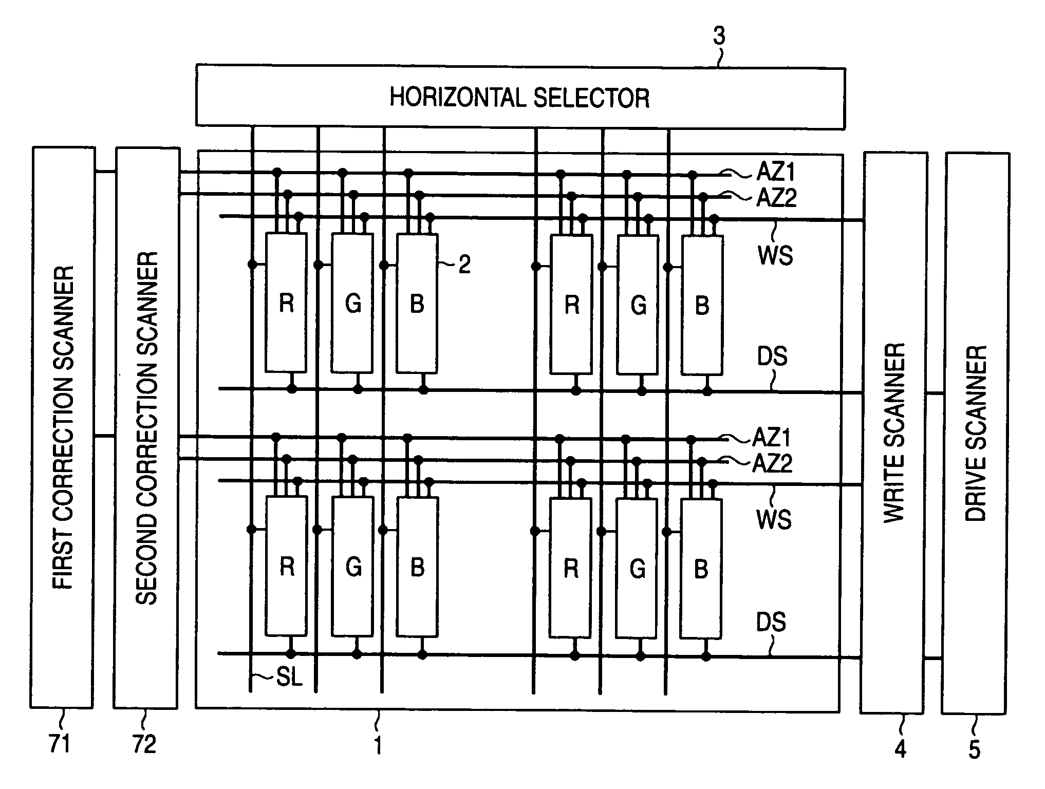
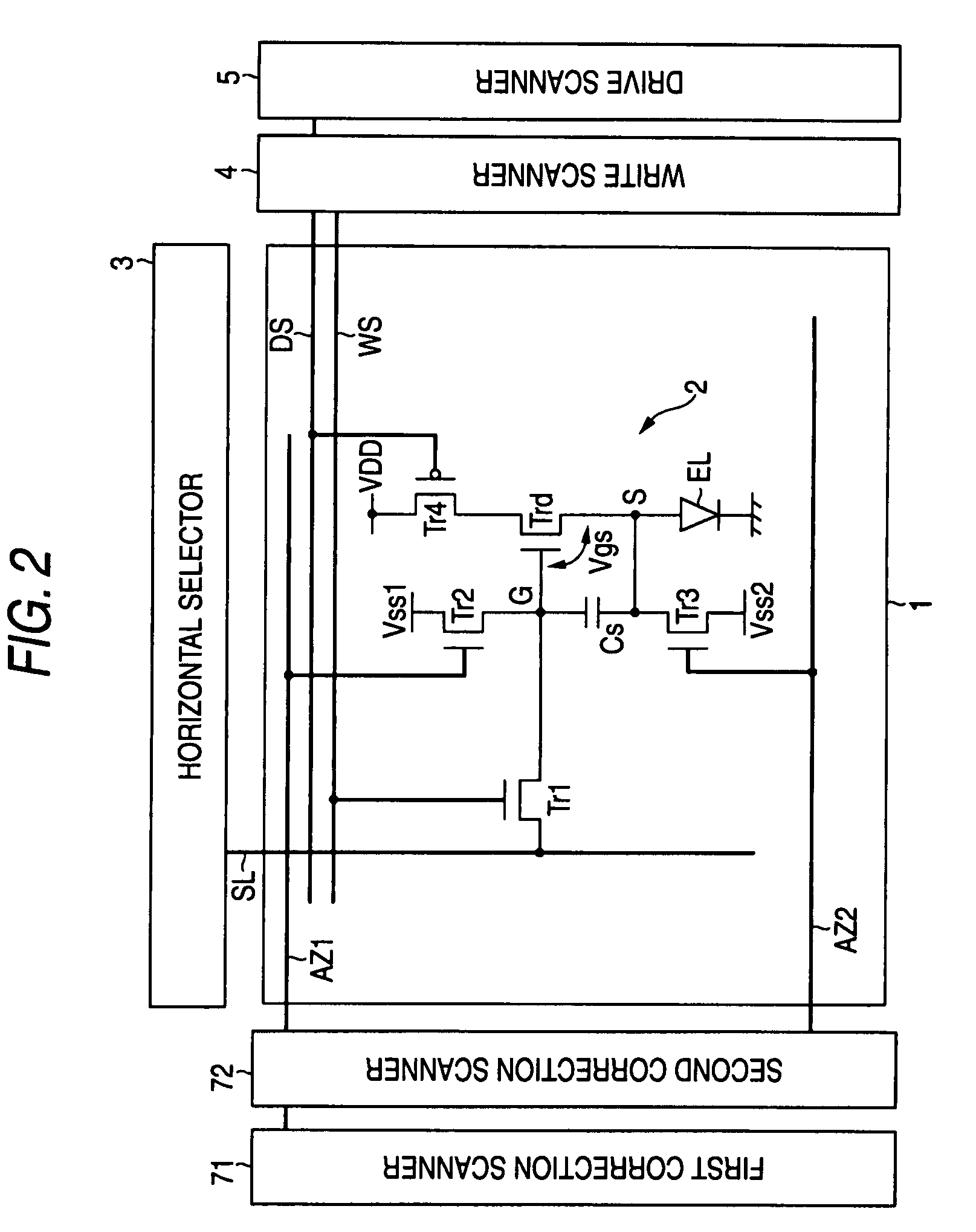
[0038]Hereinafter, an embodiment of the invention will be explained in detail with reference to the drawings. FIG. 1 is a block diagram showing the whole configuration of a display device according to an embodiment of the invention. As shown in the drawing, the display device basically includes a pixel array unit 1, a scanner unit and a signal unit. The scanner unit and the signal unit form a driving unit. The pixel array unit 1 includes first scanning lines WS, second scanning lines DS, third scanning lines AZ1 and fourth scanning lines AZ2 which are arranged in rows, signal lines SL which are arranged in columns, pixel circuits 2 in a matrix state which are connected to the scanning lines WS, DS, AZ1 and AZ2, and the signal lines SL, and a plurality of power supply lines supplying a first potential Vss1, a second potential Vss2 and a third potential VDD which are necessary for operation of respective pixel circuits 2. The signal unit includes a horizontal selector 3, which supplie...


PUM


Abstract

A display device is disclosed. The display device includes: a pixel array unit and a driving unit which drives the pixel array unit. The pixel array unit includes rows of first scanning lines and second scanning lines, columns of signals, pixels in a matrix state arranged at portions where the scanning lines and the signal lines cross each other and power supply lines and ground lines supplying power to respective pixels. The driving unit includes a first scanner performing line-sequential scanning to pixels by each row by supplying a first control signal to each first scanning line sequentially, a second scanner supplying a second control signal to each second scanning line sequentially so as to correspond to the line-sequential scanning and a signal selector supplying a video signal to rows of signal lines so as to correspond to the line-sequential scanning.

Description

CROSS REFERENCE TO RELATED APPLICATIONS[0001]The present invention contains subject matter related to Japanese Patent Application JP 2006-212579 filed in the Japanese Patent Office on Aug. 3, 2006, the entire contents of which being incorporated herein by reference.BACKGROUND OF THE INVENTION[0002]1. Field of the Invention[0003]The invention relates to a display device displaying pictures by driving light emitting elements by current, which are arranged at each pixel. Particularly, the invention relates to a so-called active matrix display device which controls a current amount flowing in the light emitting element such as an organic EL by an insulated-gate field effect transistor provided in each pixel circuit. In addition, the invention relates to electronic equipment in which such display device is incorporated.[0004]2. Description of the Related Art[0005]In a display device, for example, in a liquid crystal display, a lot of liquid crystal pixels are arranged in a matrix state, ...

Claims


Application Information

Patent Timeline
Patent Type & Authority Patents(United States)
IPC IPC(8): G09G3/30
CPCG09G3/3233G09G3/30G09G2300/043G09G2300/0819G09G2300/0842G09G2360/147G09G2320/0233G09G2320/043G09G2300/0861G09G2300/0408G09G2310/08
Inventor YAMASHITA, JUNICHITANIKAME, TAKAOUCHINO, KATSUHIDE
Owner SONY CORP
Why Eureka
Try Eureka