
Vernier delay circuit

a delay circuit and delay technology, applied in the direction of pulse manipulation, pulse automatic control, pulse technique, etc., can solve the problem of unreachable resolution and achieve the effect of high-precision calibration

Inactive Publication Date: 2010-11-09
ADVANTEST CORP
View PDF8 Cites 14 Cited by
  • Summary
  • Abstract
  • Description
  • Claims
  • Application Information

AI Technical Summary

Benefits of technology

[0014]The present invention addresses the problem and a purpose thereof is to provide a Vernier delay circuit that allows highly precise calibration.
[0016]In a Vernier delay circuit, the absolute precision of the first delay amount t1 provided by the first variable delay element in each stage and the second delay amount t2 provided by the second variable delay element is not called for. What is needed is to maintain a difference between the delay amounts (hereinafter, referred to as differential delay) Δt=(t1−t2) at a constant level. Therefore, the differential delay Δt in each stage is brought to a target level, using the individual bias circuit, while canceling variation in the delay amounts t1 and t2 due to temperature variation and power supply variation, using the bias signal from the bias signal adjusting unit. Accordingly, highly precise calibration is achieved.
[0025]According to this embodiment, a differential delay Δt in each stage of a Vernier delay circuit is maintained at a target level. Therefore, high time resolution is achieved.

Problems solved by technology

Accordingly, there is a problem in that a desired resolution is not achieved when the delay amount provided by the first delay element D1 or the second delay element D2 fluctuates or varies due to fluctuation in the process, temperature, or power supply voltage.

Method used


Image

  • Vernier delay circuit
  • Vernier delay circuit
  • Vernier delay circuit

Examples


first embodiment

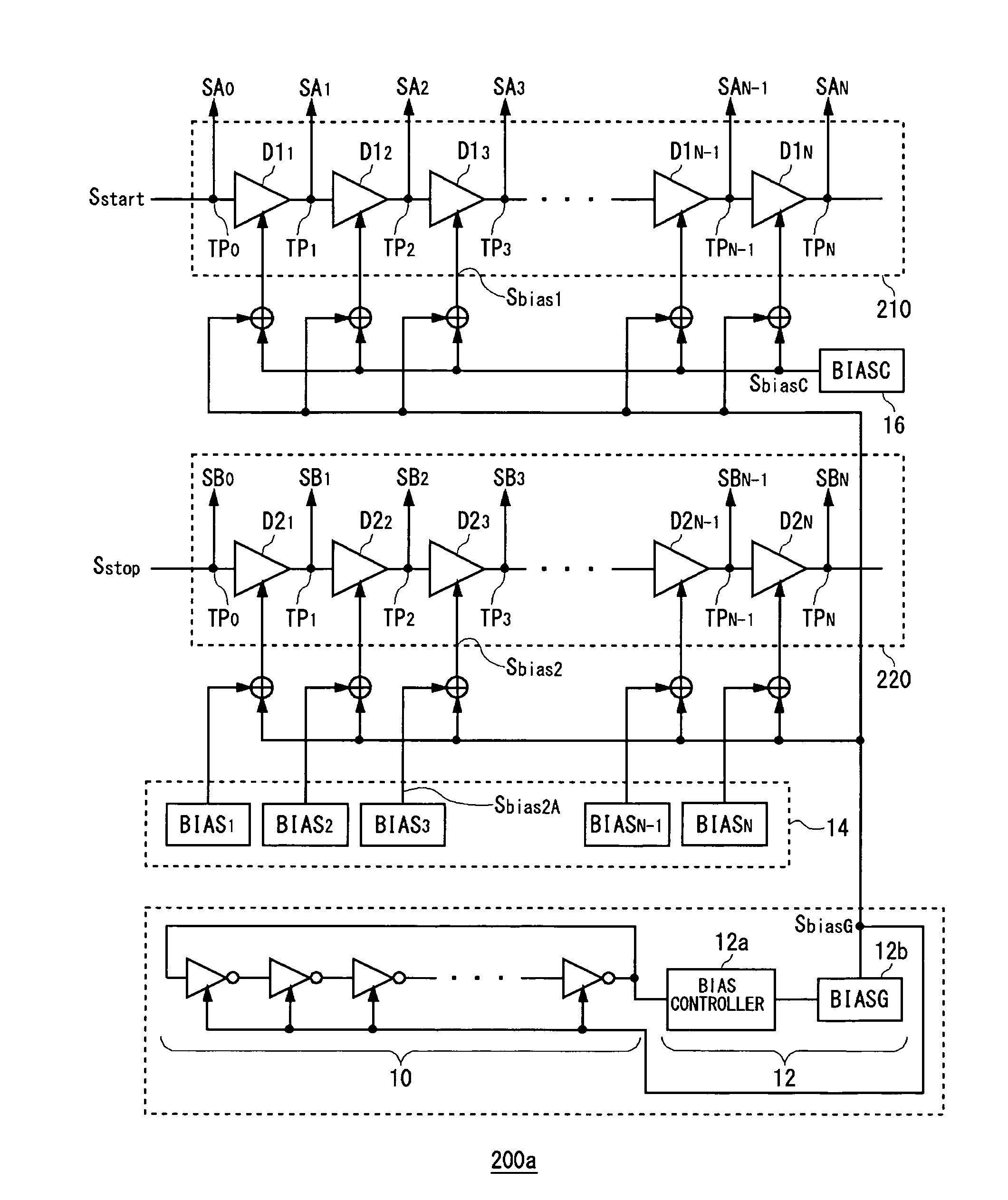
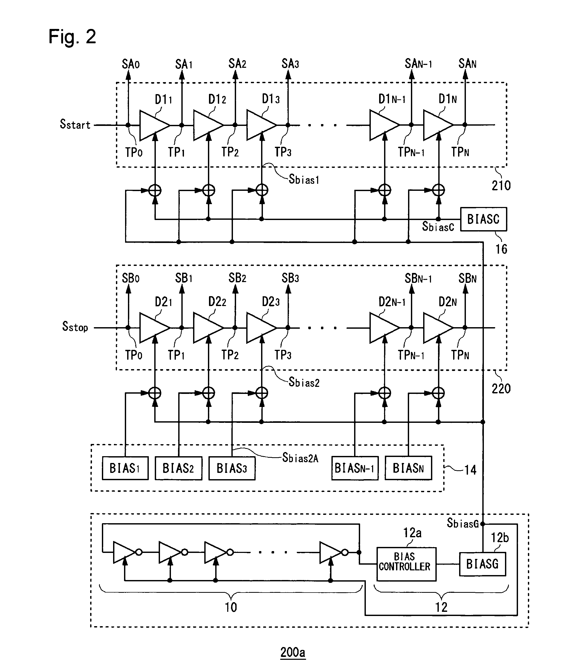
[0038]FIG. 2 is a block diagram showing the structure of a Vernier delay circuit 200a according to the first embodiment. The Vernier delay circuit 200a is suitably used in the TDC 300 of FIG. 1. The TDC 300 is provided in test apparatuses like automatic test equipment (ATE), time interval analyzers, and jitter measuring devices.

[0039]The Vernier delay circuit 200a of FIG. 2 receives a start signal (first signal) Sstart and a stop signal (second signal) Sstop and provides different multi-stage delays to the two signals.

[0040]The Vernier delay circuit 200 comprises a first delay circuit 210, a second delay circuit 220, a ring oscillator 10, a bias signal adjusting unit 12, an individual bias circuit 14, and a common bias circuit 16.

[0041]The first delay circuit 210 includes a total of N first variable delay elements D11-D1N connected to form multiple stages, where N denotes a natural number. The variable delay elements D11-D1N provide a delay determined by bias signals Sbias11-Sbias1N...

second embodiment

[0059]In addition to the function of the Vernier delay circuit 200a, the Vernier delay circuit 200b according to the second embodiment is provided with the function of suitably calibrating the differential delay Δt.

[0060]FIG. 6 is a circuit diagram showing the structure of the Vernier delay circuit 200b according to the second embodiment. FIG. 6 does not show the ring oscillator 10 or the bias signal adjusting unit 12.

[0061]In addition to the features of the Vernier delay circuit 200a of FIG. 2, the Vernier delay circuit 200b comprises a first tap selector 20, a second tap selector 22, a loop input selector 24, a frequency counter 26, an inverter 28, a first input selector 30, a second input selector 32, and a controller 34.

[0062]The first tap selector 20 receives a plurality of first delayed start signals SA0-SAN output from the first delay circuit 210, and selects and outputs one of the signals. The second tap selector 22 receives the plurality of second delayed start signals SB0-...


PUM


Abstract

A ring oscillator oscillates at a frequency determined by an input bias signal. A bias signal adjusting unit produces a bias signal for the ring oscillator using feedback so that the oscillation frequency of the ring oscillator matches a predetermined reference frequency. An individual bias circuit includes a plurality of bias circuits provided for a total of N second variable delay elements, respectively. The bias circuits are configured such that the bias signals can be individually adjusted.

Description

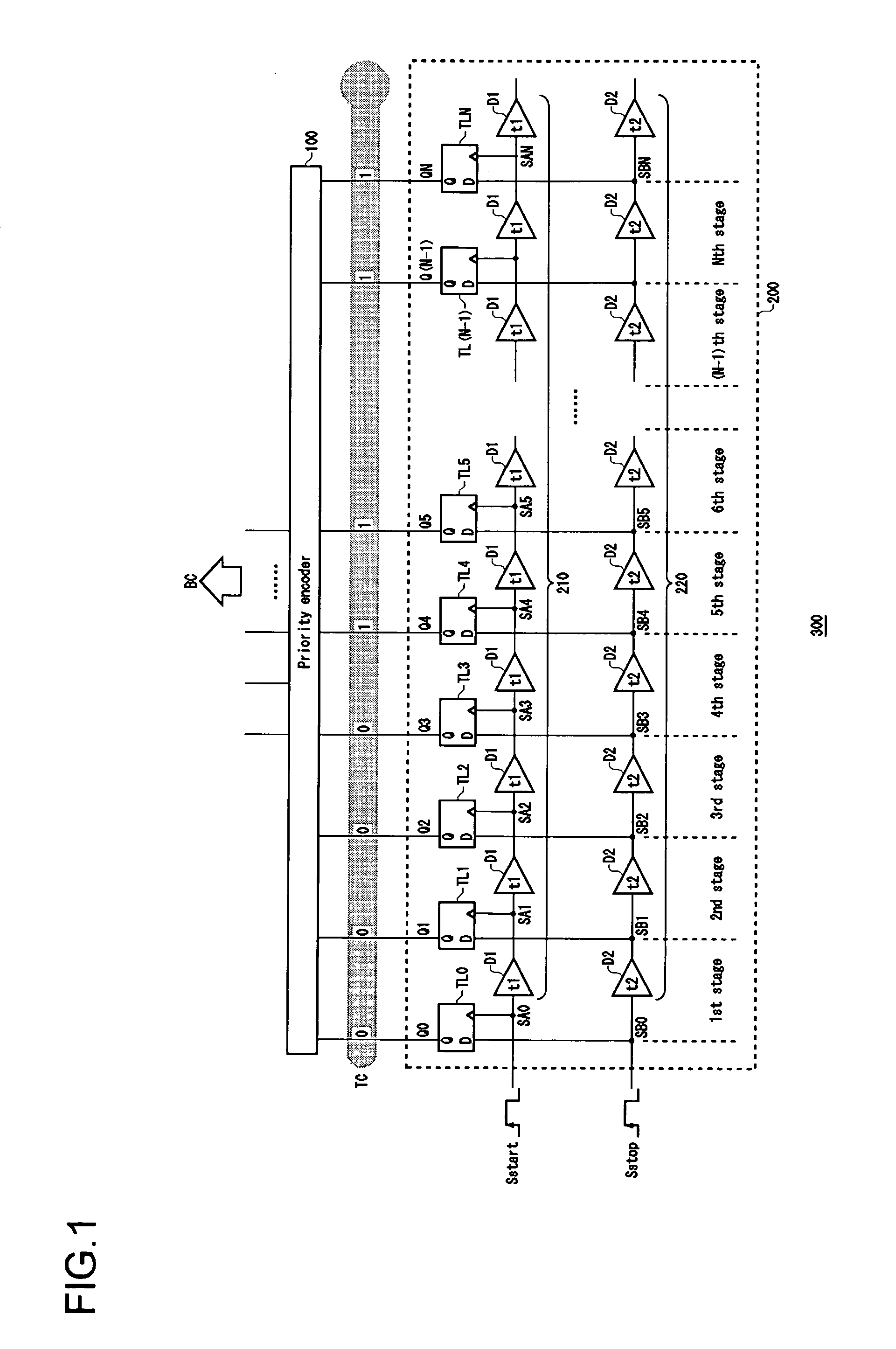
[0001]The present application is claiming priority of Japanese Patent Application No. 2008-088016, filed on Mar. 28, 2008, the content of which is incorporated herein by reference.BACKGROUND OF THE INVENTION[0002]1. Field of the Invention[0003]The present invention relates to a Vernier delay circuit and, more particularly, to a technology for adjusting a delay time.[0004]2. Description of the Related Art[0005]A time to digital converter (hereinafter, referred to as TDC) is known as a device to convert a time difference that occurs between the timing of transition of a first signal (hereinafter, referred to as a start signal) and the timing of transition of a second signal (stop signal) into a digital value. The scheme using a Vernier delay circuit in a TDC to achieve high time resolution is proposed.[0006]FIG. 1 shows the structure of a TDC 300 where a Vernier delay circuit 200 is used. The TDC 300 comprises a Vernier delay circuit 200 and a priority encoder 100. The Vernier delay c...

Claims


Application Information

Patent Timeline
Patent Type & Authority Patents(United States)
IPC IPC(8): H03H11/26H03K5/13H03L7/00
CPCH03K5/131H03L7/0805H03L7/0995H03K2005/00052H03K2005/00065
Inventor KOJIMA, SHOJISUDA, MASAKATSU
Owner ADVANTEST CORP
Learn More