Jitter suppression circuit

a jitter suppression and circuit technology, applied in the field of jitter suppression circuits, can solve the problems of circuit scale growth, circuit components are affected, and the setting to a narrow band cannot be achieved, and achieve the effect of suppressing jitters

Inactive Publication Date: 2010-11-09
FUJITSU LTD
View PDF15 Cites 14 Cited by
  • Summary
  • Abstract
  • Description
  • Claims
  • Application Information

AI Technical Summary

Benefits of technology

[0027]It is accordingly an object of the present invention to provide a circuit which suppresses jitters without a synchronizing clock signal and a growth of a circuit scale.
[0037]According to the present invention, it becomes possible to make a synchronizing clock signal unnecessary and to suppress the jitter components within a jitter transfer bandwidth which could not be suppressed only by the broadband CDR circuit. Also, it becomes possible to perform the jitter suppression with an extremely small scale circuit and a sufficient accuracy in a header portion detection by a frame synchronous circuit used in a SONET framer circuit or the like, thereby being mounted on a compact optical transceiver such as an XFP module.

Problems solved by technology

An optical transmission circuit, in which it is required to provide a high-quality and stable optical signal independently of a waveform or the like of an electric input data signal, encounters a problem of jitter components (hereinafter, occasionally referred to as phase deviations) in the electric input data signal.
It is to be noted that setting to a narrow band can not be achieved in this case because the regenerated data may have an error due to a clock extracted by a narrowband PLL circuit when the input data signal Es with the jitter components is tapped or sampled.
Namely, in the latter case, a VCO (voltage controlled oscillator) used for the narrowband PLL circuit 9 is inevitably attached as an external part, resulting in a problem that a circuit scale grows.

Method used


Image

  • Jitter suppression circuit
  • Jitter suppression circuit
  • Jitter suppression circuit

Examples


Embodiment Construction

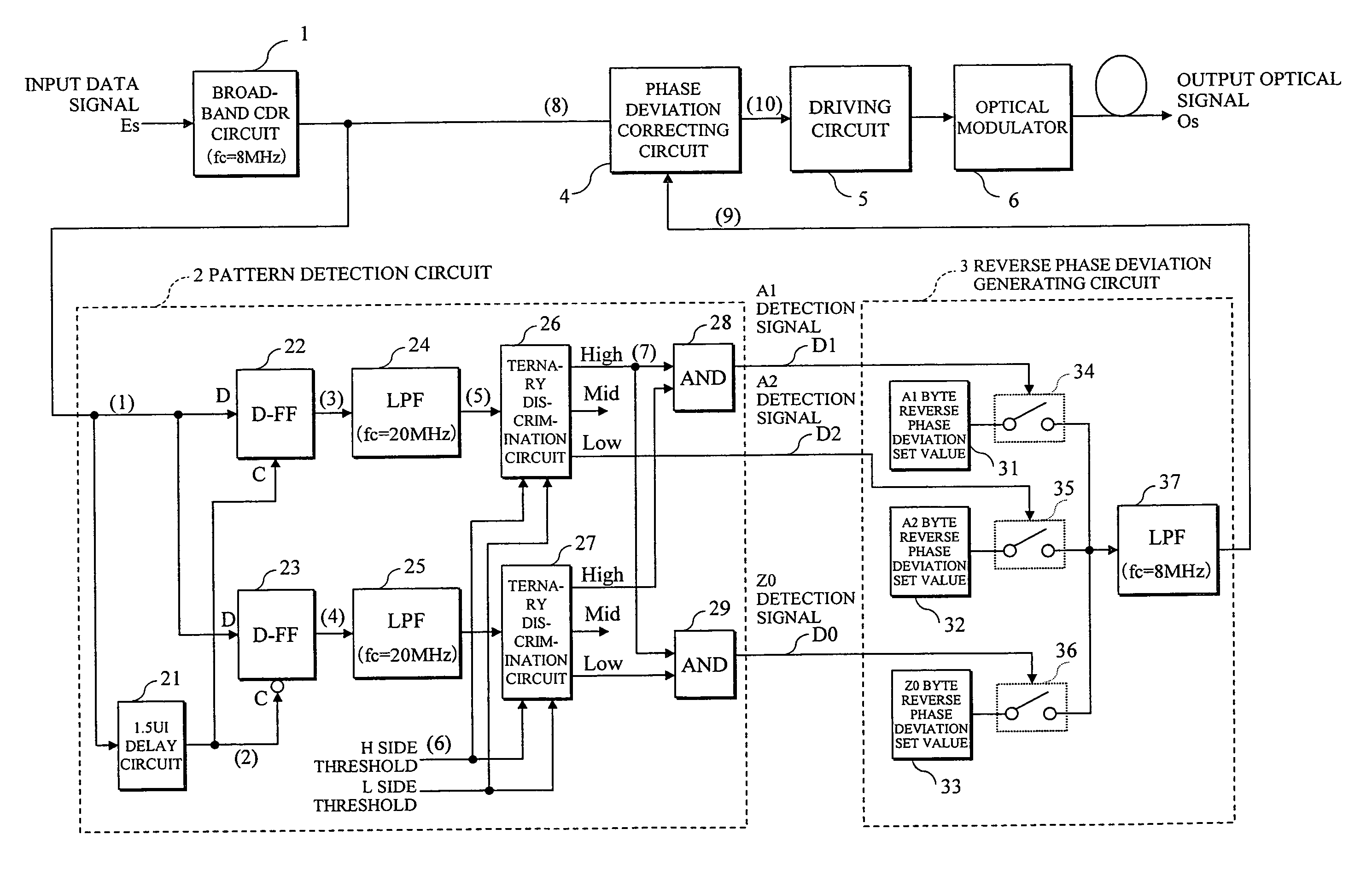
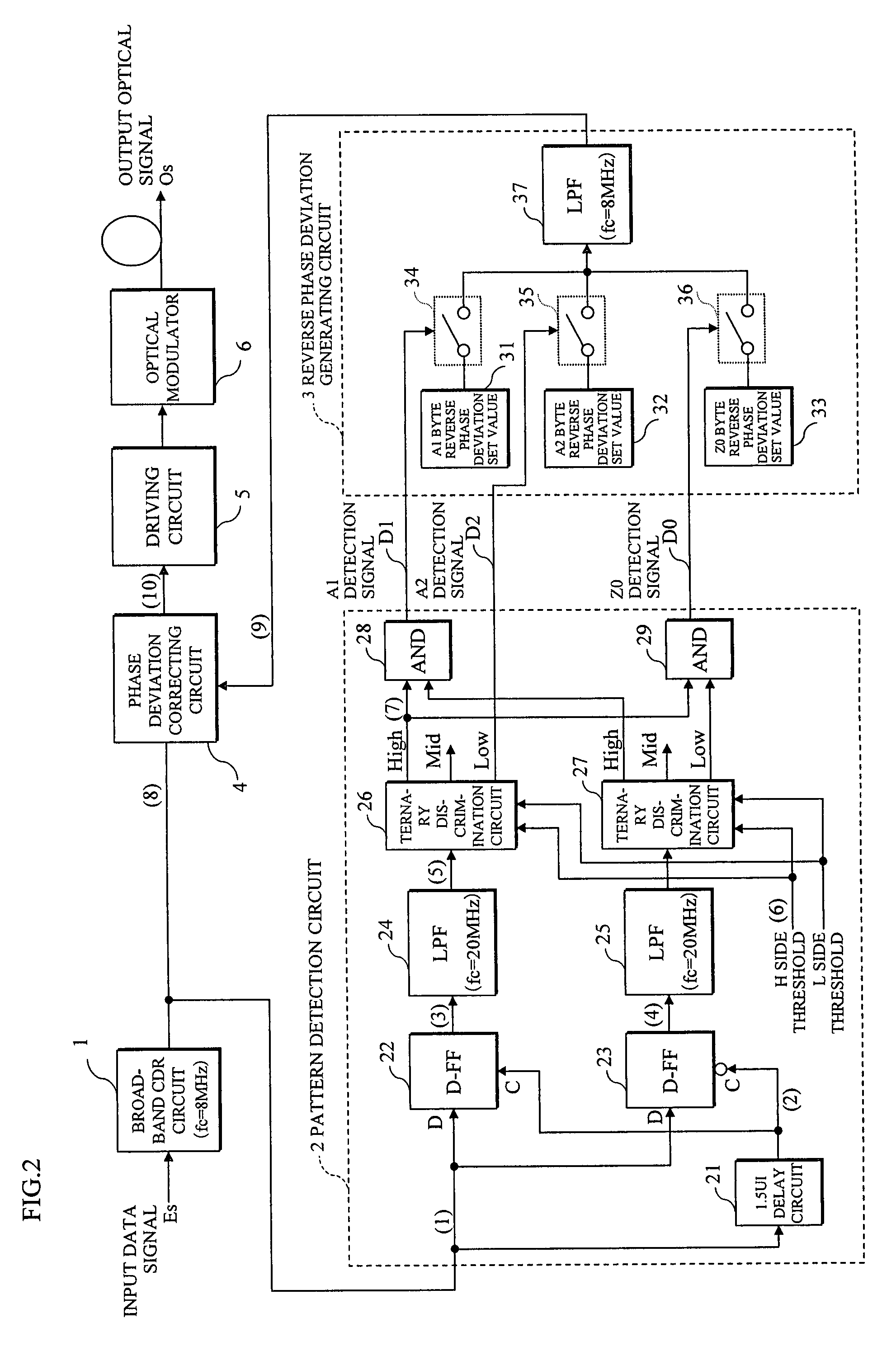
[0046]FIG. 2 shows one embodiment of the jitter suppression circuit according to the present invention conceptually shown in FIG. 1, and in particular shows a specific arrangement of the pattern detection circuit 2 and the reverse phase deviation generating circuit 3.

Pattern Detection Circuit 2

[0047]Firstly, the pattern detection circuit 2 is schematically composed of a 1.5 UI (Unit Interval) delay circuit 21, two D-FFs 22 and 23, two lowpass filters (LPFs) 24 and 25, two ternary discrimination circuits 26 and 27, and two AND gates 28 and 29.

[0048]In this pattern detection circuit 2, output data (1) of the broadband CDR circuit 1 is commonly provided to the 1.5 UI delay circuit 21 and the D-FFs 22 and 23. The 1.5 UI delay circuit 21 provides, after having delayed the output data of the broadband CDR circuit 1 by the period of 1.5 times a clock period, the output data as it is to the D-FF 22 as a clock signal (2), and provides to the D-FF 23 the clock signal (2) in the inverted form....


PUM


Abstract

In a circuit suppressing jitters without a synchronizing clock signal and an increase of a circuit scale, input data is regenerated by a data regeneration circuit in a broadband, a predetermined signal pattern which generates phase deviations exceeding a predetermined value is detected from the data regenerated by the data regeneration circuit by a pattern detection circuit, a reverse phase deviation signal having reverse phase deviations of phase deviations corresponding to the predetermined signal pattern is generated by a reverse phase deviation generating circuit, and an output signal of the data regeneration circuit is canceled by a phase deviation correcting circuit with the reverse phase deviation signal.

Description

CROSS-REFERENCE TO RELATED APPLICATION[0001]This application is a continuation of International Application PCT / JP2005 / 005029 filed on Mar. 18, 2005, the contents of which are herein wholly incorporated by reference.BACKGROUND OF THE INVENTION[0002]1. Field of the Invention[0003]The present invention relates to a jitter suppression circuit, and in particular to a jitter suppression circuit for suppressing jitter components which occur when an optical output signal is provided from an electric input data signal in an optical transmission circuit.[0004]2. Description of the Related Art[0005]An optical transmission circuit, in which it is required to provide a high-quality and stable optical signal independently of a waveform or the like of an electric input data signal, encounters a problem of jitter components (hereinafter, occasionally referred to as phase deviations) in the electric input data signal. The jitter components will now be briefly described.[0006]FIG. 5A shows a format ...

Claims


Application Information

Patent Timeline
Patent Type & Authority Patents(United States)
IPC IPC(8): H04L7/00H04L25/00H04L25/40
CPCH04J3/0608H04L7/0091
Inventor KUWATA, NAOKI
Owner FUJITSU LTD
Why Eureka
Try Eureka