Dual band photodetector

a photodetector and dual band technology, applied in the field of photodetectors, can solve the problems of limited application range of all the presently available detectors in this spectral range, limited application range of 1 w, and inability to expand the array format easily

Active Publication Date: 2010-11-23
GEORGIA STATE UNIV RES FOUND INC
View PDF27 Cites 15 Cited by
  • Summary
  • Abstract
  • Description
  • Claims
  • Application Information

AI Technical Summary

Problems solved by technology

All the presently available detectors in this spectral range have limitations on their operation.
However, typical intensity limits of 1 W restrict applications.
Thus, such Golay cell are not readily extended to array formats.
In addition, being thermal detectors, they will have very slow response times. Further, although a Keating meter, which has a typical area of 30 cm2, will provide an absolute calibration, it is slow, requires a modulated signal (10-50 Hz), and cannot be converted into an array format with high resolution.
And, while bolometer detectors can achieve high sensitivities (>105 V / W) by cooling to low temperatures, they are not very fast.
However, the stress requirements of the Ge:Ga detectors make them relatively unsuited for use in array formats.
Thus, although several THz detectors are available in the market, each has its limitations.

Method used


Image

  • Dual band photodetector
  • Dual band photodetector
  • Dual band photodetector

Examples


Embodiment Construction

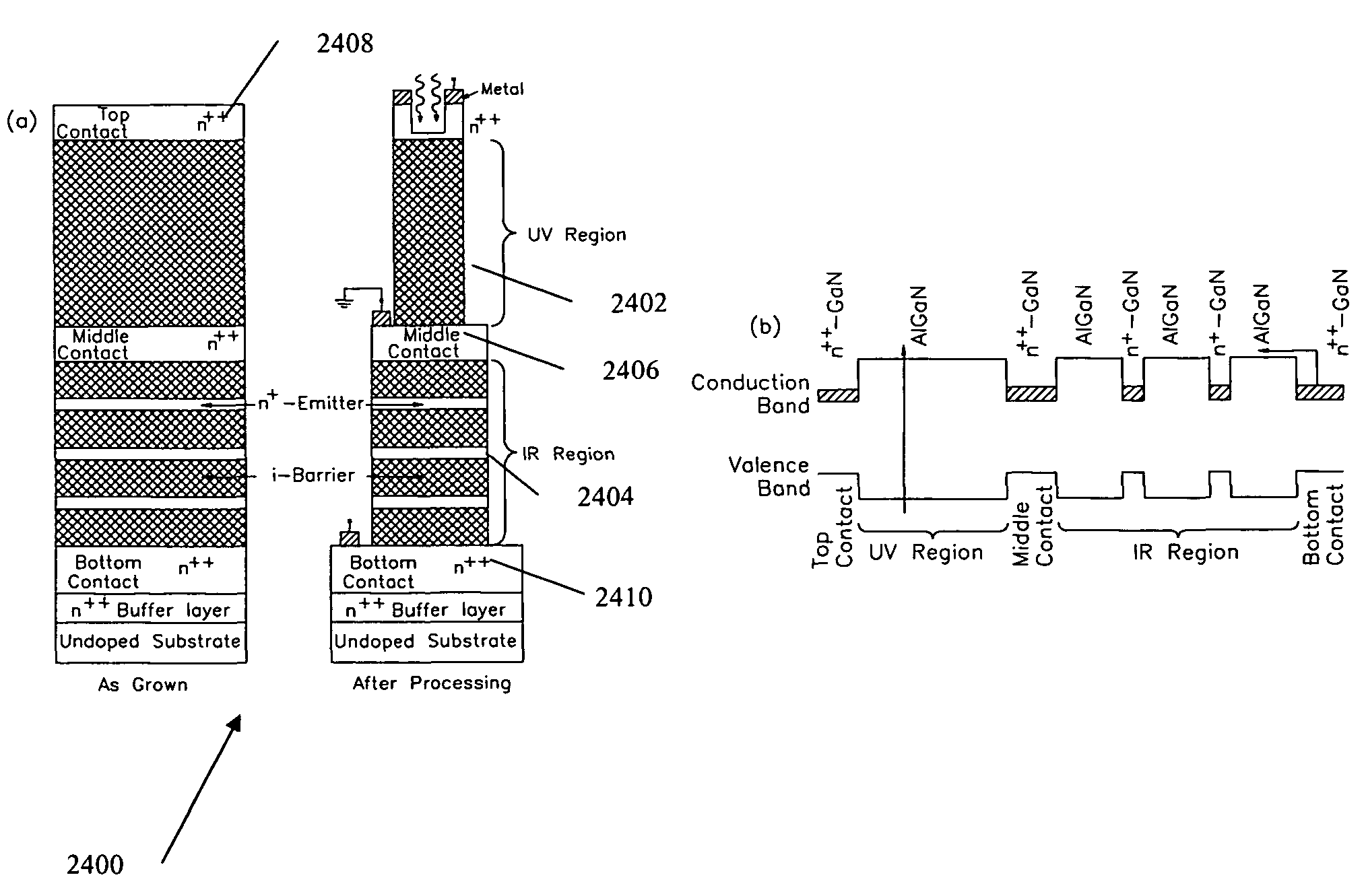
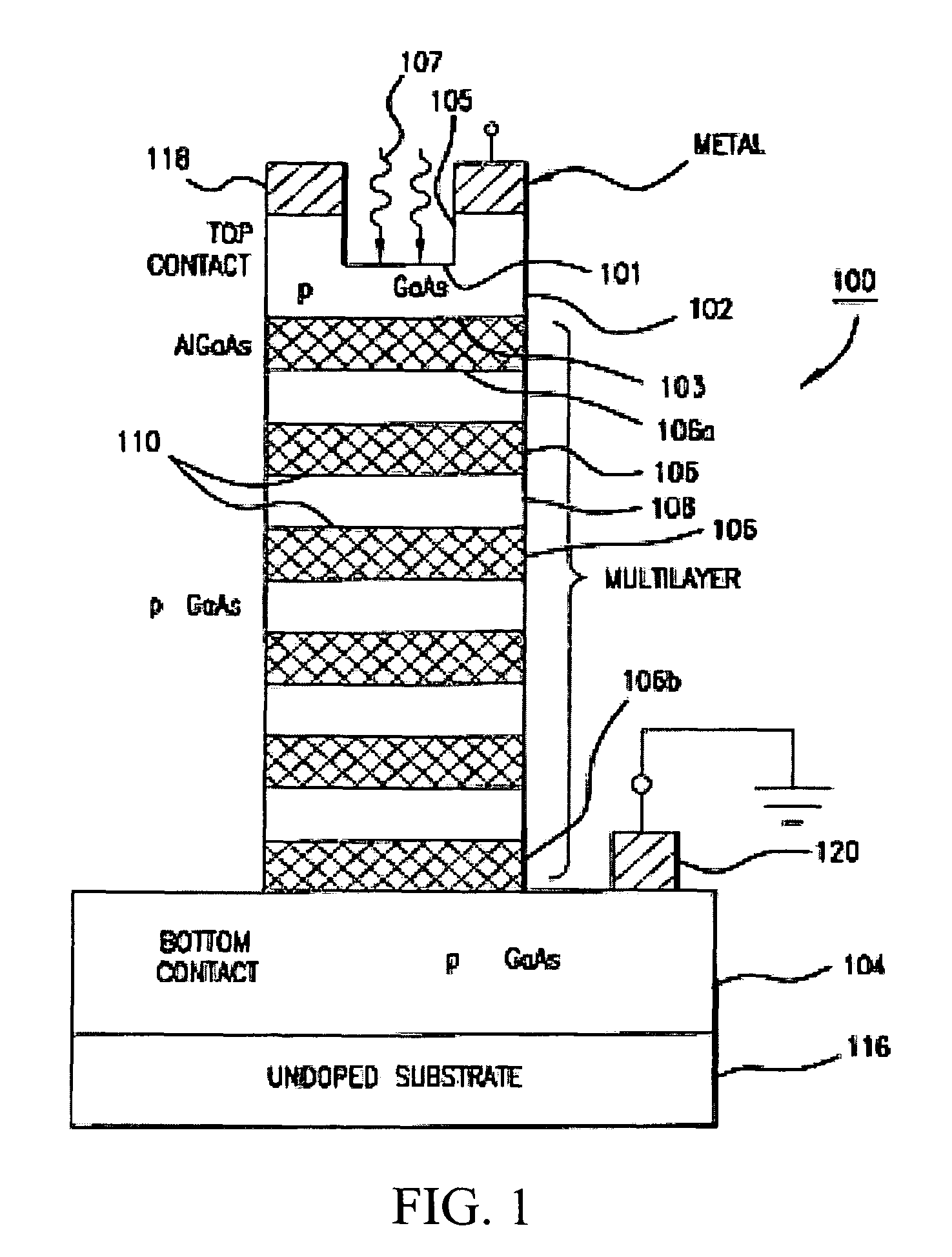
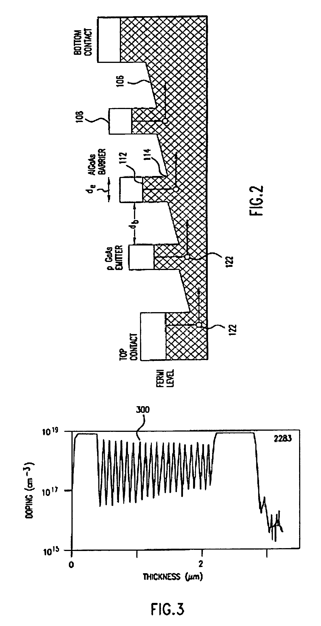
[0082]Several embodiments of the invention are now described in detail. Referring to the drawings, like numbers indicate like parts throughout the views. As used in the description herein and throughout the claims that follow, the meaning of “a,”“an,” and “the” includes plural reference unless the context clearly dictates otherwise. Also, as used in the description herein and throughout the claims that follow, the meaning of “in” includes “in” and “on” unless the context clearly dictates otherwise.

[0083]Additionally, as used in the description herein and throughout the claims that follow as known to people skilled in the art, a homojunction means a junction formed by two different electrical types of the same (band-gap) material. For example, a silicon p-n junction is a homojunction. A heterojunction means a junction formed by two different electrical types of two chemically different materials, each having a band-gap different from that of the other. An example of a heterojunction ...


PUM


Abstract

A dual band photodetector for detecting infrared and ultraviolet optical signals is disclosed. Aspects include homojunction and heterojunction detectors comprised of one or more of GaN, AlGaN, and InGaN. In one aspect ultraviolet / infrared dual-band detector is disclosed that is configured to simultaneously detect UV and IR.

Description

CROSS-REFERENCE TO RELATED PATENT APPLICATION[0001]This application claims the benefit, pursuant to 35 U.S.C. §119(e), of the provisional U.S. Patent Application Ser. No. 60 / 729,163 filed Oct. 21, 2005, entitled “Heterojunction Photodetector,” which application is hereby incorporated by reference in its entirety and made a part hereof.ACKNOWLEDGEMENTS[0002]This invention was made with government support under one or more of Grants ECS-0140434, ECS-0553051 and DBI: 0352324 awarded by the National Science Foundation (NSF); and Grants No. FA9453-05-M-0106 awarded by the U.S. Air Force Small Business Innovation Research Program (SBIR). The government has certain rights in the invention.BACKGROUND OF THE INVENTION[0003]1. Field of the Invention[0004]The present invention generally relates to a photodetector. More particularly, the present invention relates to a far infrared photodetector utilizing a mechanism of detection based on free carrier absorption and internal photoemission over t...

Claims


Application Information

Patent Timeline
Patent Type & Authority Patents(United States)
IPC IPC(8): H01L29/06
CPCB82Y20/00H01L31/035236H01L31/103
Inventor PERERA, A.G. UNILMATSIK, STEVEN GEORGE
Owner GEORGIA STATE UNIV RES FOUND INC
Why Eureka
Try Eureka