Method and system for providing a structure in a microelectronic device using a chromeless alternating phase shift mask

Inactive Publication Date: 2010-12-07
WESTERN DIGITAL TECH INC
View PDF14 Cites 148 Cited by
  • Summary
  • Abstract
  • Description
  • Claims
  • Application Information

AI Technical Summary

Benefits of technology

[0008]FIG. 1 is a flow chart depicting a conventional method for providing a convention

Problems solved by technology

Although the conventional method 10 may be used for microelectric devices, such as read transducers, there are drawbacks.
However, the co

Method used


Image

  • Method and system for providing a structure in a microelectronic device using a chromeless alternating phase shift mask
  • Method and system for providing a structure in a microelectronic device using a chromeless alternating phase shift mask
  • Method and system for providing a structure in a microelectronic device using a chromeless alternating phase shift mask

Examples


Embodiment Construction

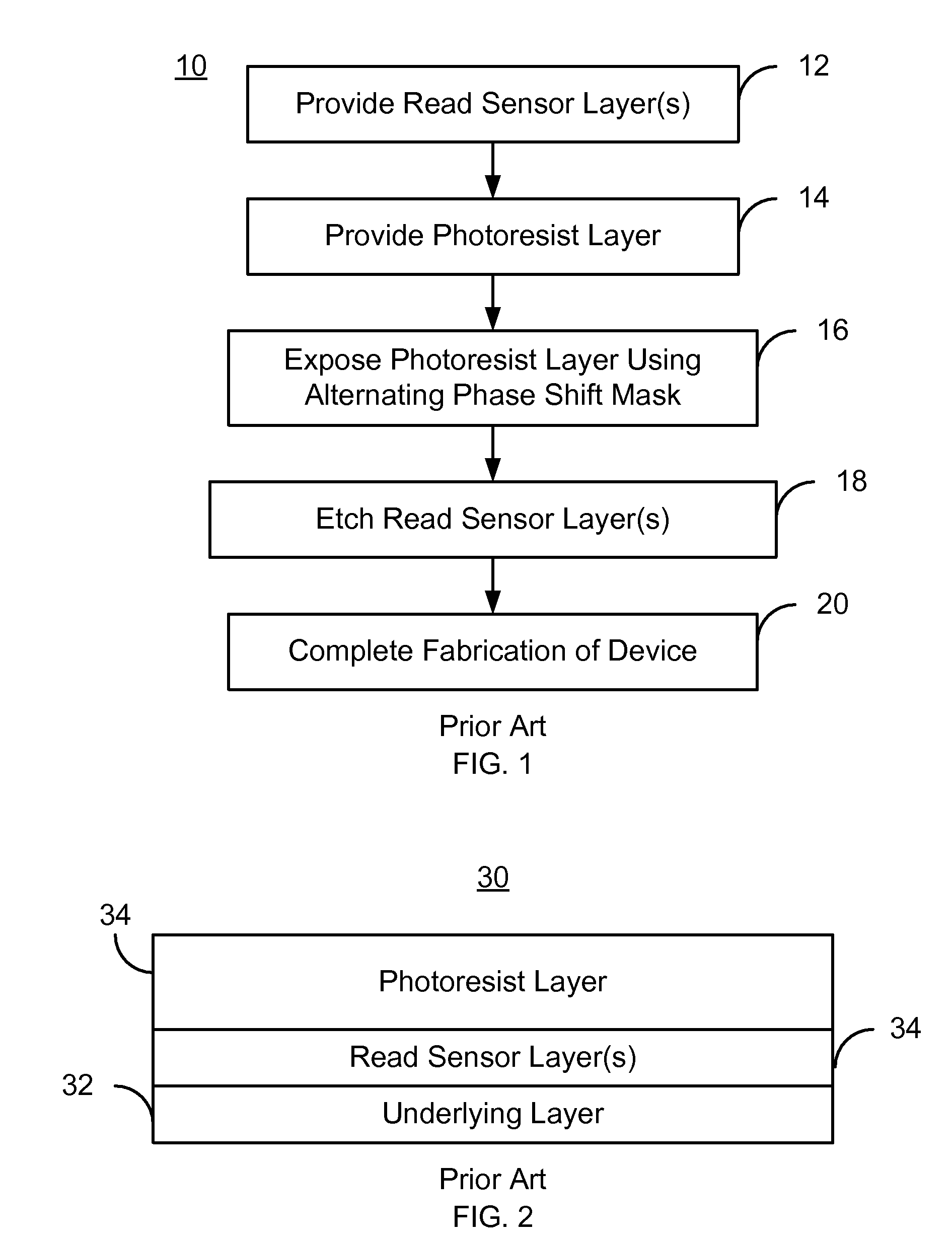
[0024]FIG. 9 is a flow chart depicting an exemplary embodiment of a method 100 for fabricating a structure in a microelectric device, such as a read transducer. For simplicity, some steps in the method 100 may be omitted. In addition, other and / or additional steps not inconsistent with the method and system may be used. The method 100 is described in the context of defining a read sensor of a read transducer. However, in another embodiment, the method 100 may be used in providing another structure that may be in another type of head and / or another type of microelectric device. For example, the method 100 may be used in providing a conductive line.

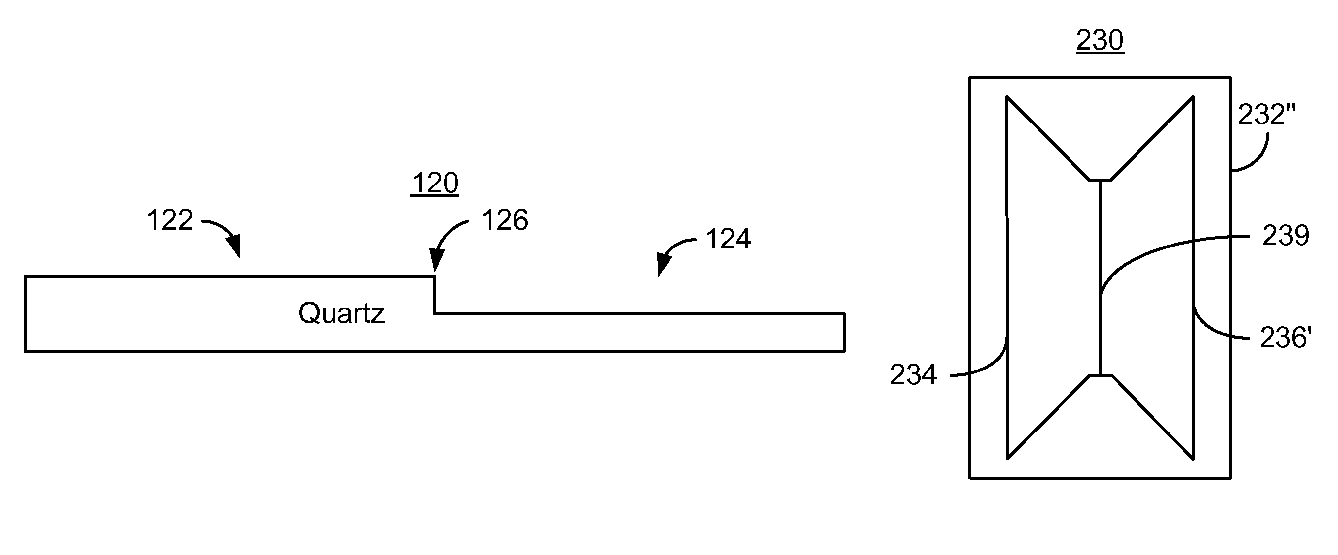
[0025]The method 100 is also described in the context of FIGS. 10-15. FIGS. 10-11 depict an exemplary embodiment of a microelectric device 110 during fabrication using the method 100. FIGS. 12-13 depict side and plan views of an exemplary embodiment of a chromeless alternating phase shift mask (chromeless alt-PSM) 120 used in the method 100...


PUM


Abstract

A method and system for providing a microelectric device, such as a magnetoresistive read sensor are described. The method and system include providing a mask layer on the microelectric device. The method and system further include exposing the mask layer to provide a mask. A portion of the mask covers a portion of the microelectric device. The step of exposing the mask layer further includes utilizing a chromeless alt-phase shift mask for providing the portion of the mask.

Description

BACKGROUND[0001]FIG. 1 depicts a conventional method 10 for fabricating a structure, such as a read sensor, in a conventional microelectric device such as a read transducer. For clarity, therefore, the method 10 is described in the context of providing a read sensor in a read transducer. FIGS. 2-4 depict the conventional read transducer 30 during fabrication using the conventional method 10. FIGS. 5-6 depict plan and side views of the alternating phase shift mask (alt-PSM) 40 used in the conventional method 10. FIGS. 7-8 depict the field 50 and intensity 60 during fabrication using the conventional method 10. For clarity, FIGS. 2-8 are not to scale.[0002]Referring to FIGS. 1-8, layers for the read sensor are fabricated on an underlying substrate, via step 12. A photoresist layer is provided on the read sensor layer(s), via step 14. The photoresist layer is assumed to be a positive photoresist, in which areas exposed to light are removed. FIG. 2 depicts the microelectric device 30 af...

Claims


Application Information

Patent Timeline
IPC IPC(8): G03F1/00
CPCB82Y25/00G01R33/093G03F1/30G03F1/34G11B5/3906
Inventor SUN, HAIYU, WINNIEYUAN, HONGPINGWANG, YIZHONGZENG, XIANZHONG
Owner WESTERN DIGITAL TECH INC
Why Eureka
Try Eureka