
Planar programmable metallization memory cells

a metallization memory and programmable technology, applied in the direction of bulk negative resistance effect devices, electrical devices, semiconductor devices, etc., can solve the problem of uneven diffusion of metal ions

Inactive Publication Date: 2010-12-07
SEAGATE TECH LLC
View PDF9 Cites 0 Cited by
  • Summary
  • Abstract
  • Description
  • Claims
  • Application Information

AI Technical Summary

Benefits of technology

"This patent is about programmable conductor dynamic random access memories that use a programmable metallization cell. The cell has an inert electrode and an active electrode, with a fast ion conductor material in between them. The fast ion conductor includes superionic clusters that extend from the inert electrode to the active electrode. A metal layer also extends from the inert electrode to the active electrode, but is insulated from them by the fast ion conductor material. The technical effect of this patent is to provide a programmable metallization cell that allows for the creation of more efficient and reliable memories."

Problems solved by technology

Since the metal layer is positioned on one side of the memory cell, proximate the active electrode, the diffusion of the metal ions is not uniform from the top to the bottom of the PMC.

Method used


Image

  • Planar programmable metallization memory cells
  • Planar programmable metallization memory cells
  • Planar programmable metallization memory cells

Examples


first embodiment

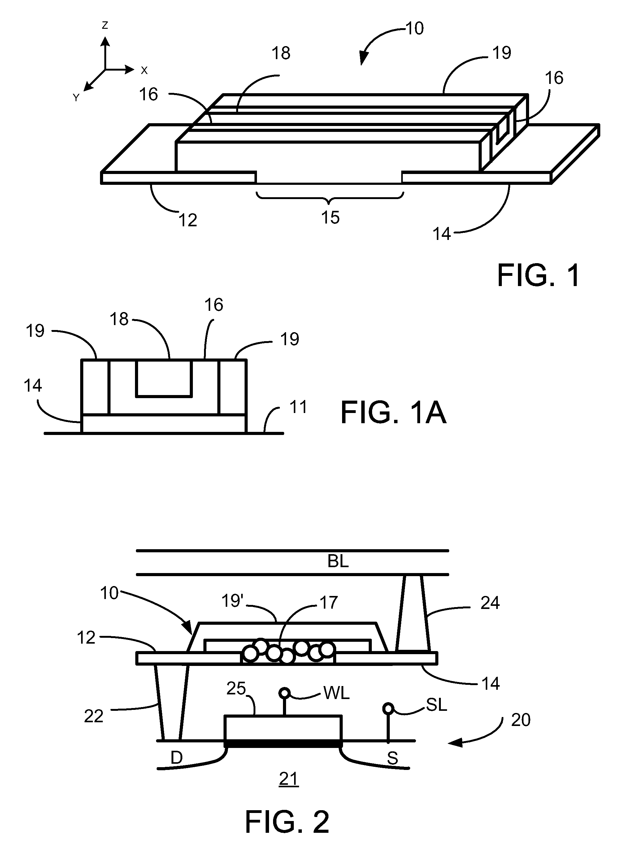
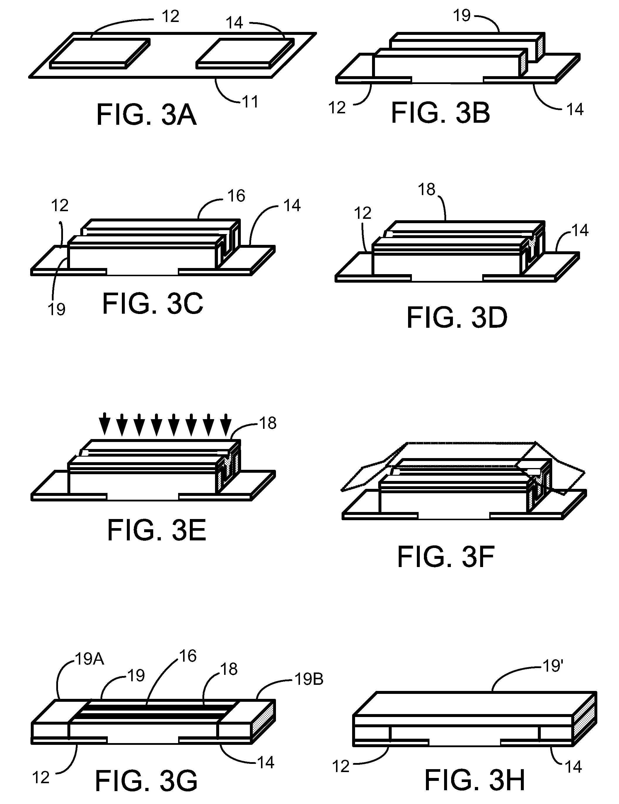
[0022]a programmable metallization memory cell according to this disclosure is illustrated in FIG. 1 and FIG. 1A as memory cell 10. Memory cell 10 has a substrate 11 with a first electrode 12 and a second electrode 14 positioned on substrate 11. Electrodes 12, 14 are co-planar, positioned on substrate 11 in a non-overlapping manner, in that no portion of one electrode (for example, electrode 12) is positioned between substrate 11 and the other electrode (for example, electrode 14). In some embodiments, electrodes 12, 14 may be non-planar, but in a non-overlapping manner.

[0023]Electrodes 12, 14 are formed of an electrically conducting material, for example, metal. First electrode 12 is an active electrode, made of for example, silver (Ag), copper (Cu), tantalum (Ta) or titanium (Ti). Second electrode 14 is an inert electrode, made of, for example, tungsten (W) or a noble metal such as gold (Au), platinum (Pt), palladium (Pd) and rhodium (Rh). Typically, the material of electrode 12 i...

second embodiment

[0036]a programmable metallization memory cell according to this disclosure is illustrated in FIGS. 4, 4A, 4B and 4C as memory cell 40. The various elements of memory cell 40 are similar to and have the same or similar properties and features as the corresponding elements of memory cell 10, unless indicated otherwise. In this embodiment, the electrodes are non-overlapping, generally co-planar, but spaced from the support substrate. Memory cell 40 has a substrate 41 with a first electrode 42 and a second electrode 44 positioned on substrate 41 with an intervening layer. Electrodes 42, 44 are positioned on substrate 41 in a non-overlapping manner, in that no portion of one electrode (for example, electrode 42) is positioned between substrate 41 and the other electrode (for example, electrode 44). Electrodes 42, 44 are parallel to substrate 41 and co-planar with each other.

[0037]Electrodes 42, 44 are formed of an electrically conducting material, for example, metal. First electrode 42 ...


PUM


Abstract

Programmable metallization memory cells that have an inert electrode and an active electrode positioned in a non-overlapping manner in relation to a substrate. A fast ion conductor material is in electrical contact with and extends from the inert electrode to the active electrode, the fast ion conductor including superionic clusters extending from the inert electrode to the active electrode. A metal layer extends from the inert electrode to the active electrode, yet is electrically insulated from each of the inert electrode and the active electrode by the fast ion conductor material. Methods for forming programmable metallization cells are also disclosed.

Description

BACKGROUND[0001]Memory devices are common in electronic systems and computers to store data. These memory devices may be volatile memory, where the stored data is lost if the power source is disconnected or removed, or non-volatile, where the stored data is retained even during power interruption. An example of a non-volatile memory device is the programmable conductor random access memory that utilizes a programmable metallization cell (PMC).[0002]A PMC utilizes a fast ionic conductor or a solid ionic electrolyte, such as a chalcogenide or oxide material, that may be embedded with a superionic phase. The PMC is oriented vertically on a substrate, as a tower or column. The fast ion conductor material or electrolyte is present between two electrodes of different reduction / oxidation potential, one electrode being an active electrode and the other an inert electrode, often composed of a noble metal. A metal layer, often silver, is positioned next to the active electrode. Superionic clu...

Claims


Application Information

Patent Timeline
Patent Type & Authority Patents(United States)
IPC IPC(8): H01L47/00H10N80/00
CPCH01L27/2436H01L45/085H01L45/1226H01L45/141H01L45/143H01L45/1658H10B63/30H10N70/245H10N70/823H10N70/882H10N70/8825H10N70/046
Inventor KHOUEIR, ANTOINEXI, HAIWENHUANG, SHUIYUAN
Owner SEAGATE TECH LLC
Learn More