Three-dimensional chip-stack synchronization

a chip-stack clock and three-dimensional technology, applied in the direction of generating/distributing signals, pulse techniques, instruments, etc., can solve the problems of critical synchronization between chips, difficulty may not necessarily extend to all chip packages, etc., to minimize clock skew and clock jitter, the effect of minimizing clock skew

Active Publication Date: 2011-01-04
INT BUSINESS MASCH CORP
View PDF4 Cites 36 Cited by
  • Summary
  • Abstract
  • Description
  • Claims
  • Application Information

AI Technical Summary

Benefits of technology

[0012]In still a further aspect of the invention, a precision clock tuning device in each child chip of the 3-D stack individually tunes the clock of each child chip. Such device can provide coarse and fine tuning of the on-chip clock regarding the central reference clock in the middle chip, and store the codes into a local register memory. During a power-on sequence, the codes are loaded to the tuning device of each child chip of the 3-D stack.
[0013]The invention further shows a formation of components of the grid, wires, through silicon vias (TSVs) and PLLs. The present invention provides a significant advance over the two dimensional H-tree clock grids known in the art by creating an analogous structure in a 3-D dimensional chip stack using TSVs or some equivalent technology elements. The value of these clock topologies is that a signal propagating from the clock PLL through the clock tree to the clock gated latches requires the clock signal to reach all the gated latches within a few picoseconds of each other. Thus, the clock skew is minimized. The minimal role for active devices or coupling to signal through passive device elements minimizes the clock skew and clock jitter, in a 3-D chip stack dependent on the TSVs using an odd number of TSVs for 2n+1 neighboring chips and an even number of TSVs for 2n neighboring chips. In addition, the invention preferably creates a delay line in series with the even number of TSVs that matches the delay associated the extra TSV on the interconnect to the 2n+1 neighbors.

Problems solved by technology

One of many difficulties with such structures is how to synchronize the clock signal among the various chips forming the stack once they are assembled.
The aforementioned difficulty may not necessarily extend to all the chip packages if the chips do not operate in a synchronous manner.
However, if each chip perform the function of a processor such as a high-speed multi-processor system or when each chip is a component of a processor, then the synchronization between the chips becomes critical.
This approach is only valid for two chips bonded face-to-face to each other, and is further limited by not being able to handle the clock skew when a plurality of chips are assembled in 3-D stack where clock signals must travel through many levels of chips and TSVs before it arrives at each chip.

Method used


Image

  • Three-dimensional chip-stack synchronization
  • Three-dimensional chip-stack synchronization
  • Three-dimensional chip-stack synchronization

Examples


Embodiment Construction

[0028]The present invention and the various features and advantageous details thereof are explained more fully with reference to the non-limiting embodiments that are illustrated in the accompanying drawings and detailed in the following description of embodiments of the invention.

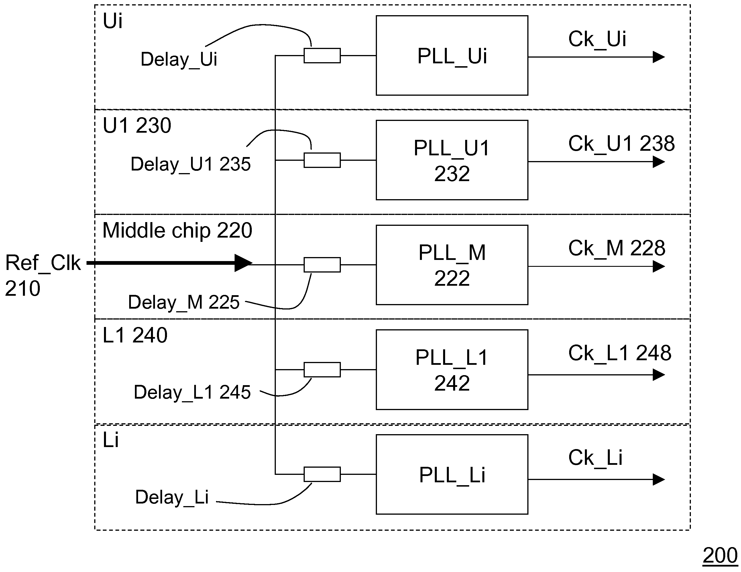
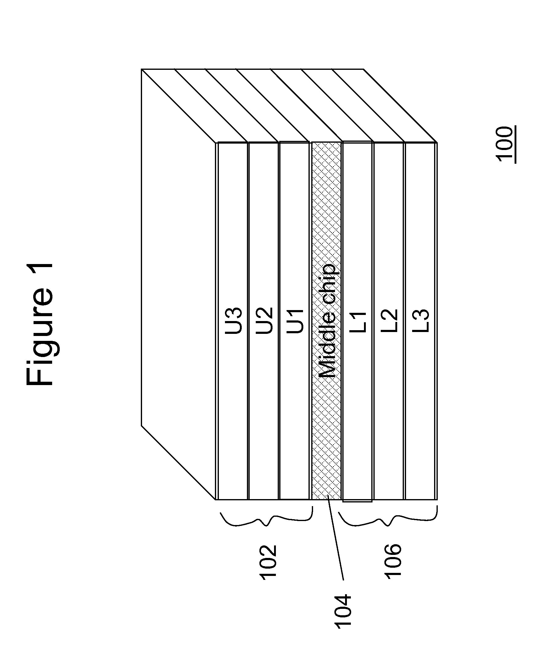
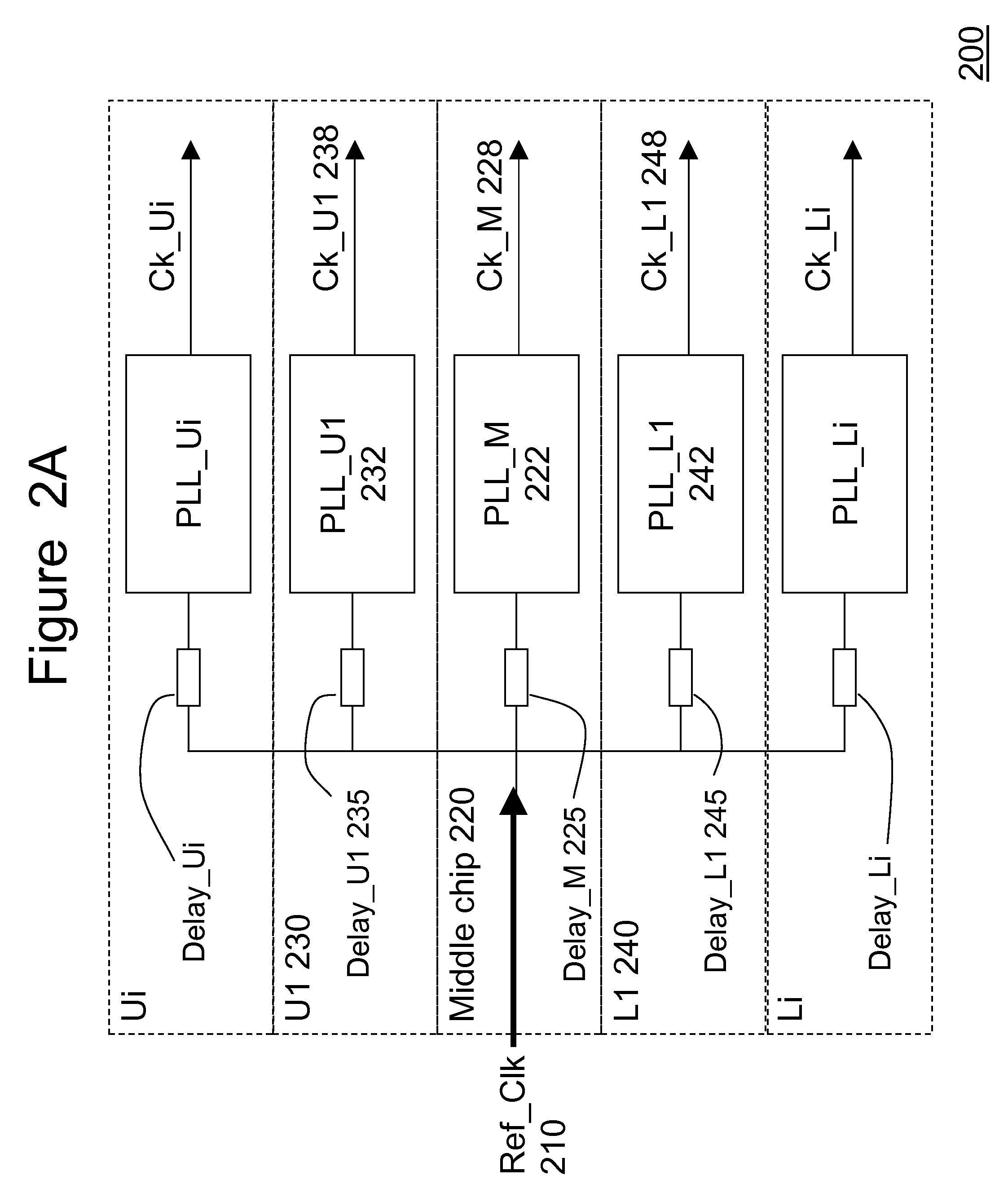
[0029]Referring to FIG. 1, there is shown an embodiment of a stacked chip structure 100. Although seven chips are shown, it is to be understood that other number of chips may be stacked to form the chip stack. In this example, a central reference clock is preferably placed in a middle chip 104 and a plurality of reference clock signals are routed to three upper chips 102 (U1, U2 and U3) (“child chip”) and three lower chips 106 (L1, L2 and L3) (“child chip”).

[0030]In general, such chips may be fabricated at the wafer level with standard devices and circuits formed in layers of the front-end of line (FEOL). Interconnects and dielectrics are then formed in layers of back-end of line (BEOL). All the chips are ...


PUM


Abstract

A central reference clock is placed in a substantially middle chip of a 3-D chip-stack. The central reference clock is distributed to each child chip of the 3-D chip-stack, so that a plurality of clocks is generated for each individual chip in the 3-D-stack in a synchronous manner. A predetermined number of through-silicon-vias and on-chip wires are employed to form a delay element for each slave clock, ensuring that the clock generated for each child chip is substantially synchronized. Optionally, an on-chip clock trimming circuit is embedded for further precision tuning to eliminate local clock skews.

Description

FIELD OF THE INVENTION[0001]The present invention relates to a clock distribution system of a microelectronic chip package, and more particularly, to a system and a method for synchronizing a three-dimension (3-D) chip-stack clock distribution.BACKGROUND AND RELATED ART[0002]In the semiconductor industry, electronic devices including semiconductor chips and wafers or semiconductor chip carriers, vertical interconnection to the next packaging level, whether chip carriers or stacked chips, may be packaged by the use of through-silicon vias (labeled TSVs). Various techniques are known to create TSVs, as well as to stack chips to form a multi-story chip structure that is sometimes referred to as a 3-D chip stack, allowing reduced die-to-die signal transmission distance and enabling a large increase in the number of links that may be established between dies.[0003]Small-sized packages, as provided by 3-D chip stacks using TSVs, are in high demand for a variety of applications, such as ce...

Claims


Application Information

Patent Timeline
Patent Type & Authority Patents(United States)
IPC IPC(8): G06F1/04
CPCH03L7/099H03L7/18H03L7/22
Inventor WANG, PING-CHUANBONACCIO, ANTHONY R.GUO, JONG-RUHSU, LOUIS LU-CHEN
Owner INT BUSINESS MASCH CORP
Why Eureka
Try Eureka