Three-dimensional chip-stack synchronization
- Summary
- Abstract
- Description
- Claims
- Application Information
AI Technical Summary
Benefits of technology
Problems solved by technology
Method used
Image
Examples
Embodiment Construction
[0028]The present invention and the various features and advantageous details thereof are explained more fully with reference to the non-limiting embodiments that are illustrated in the accompanying drawings and detailed in the following description of embodiments of the invention.
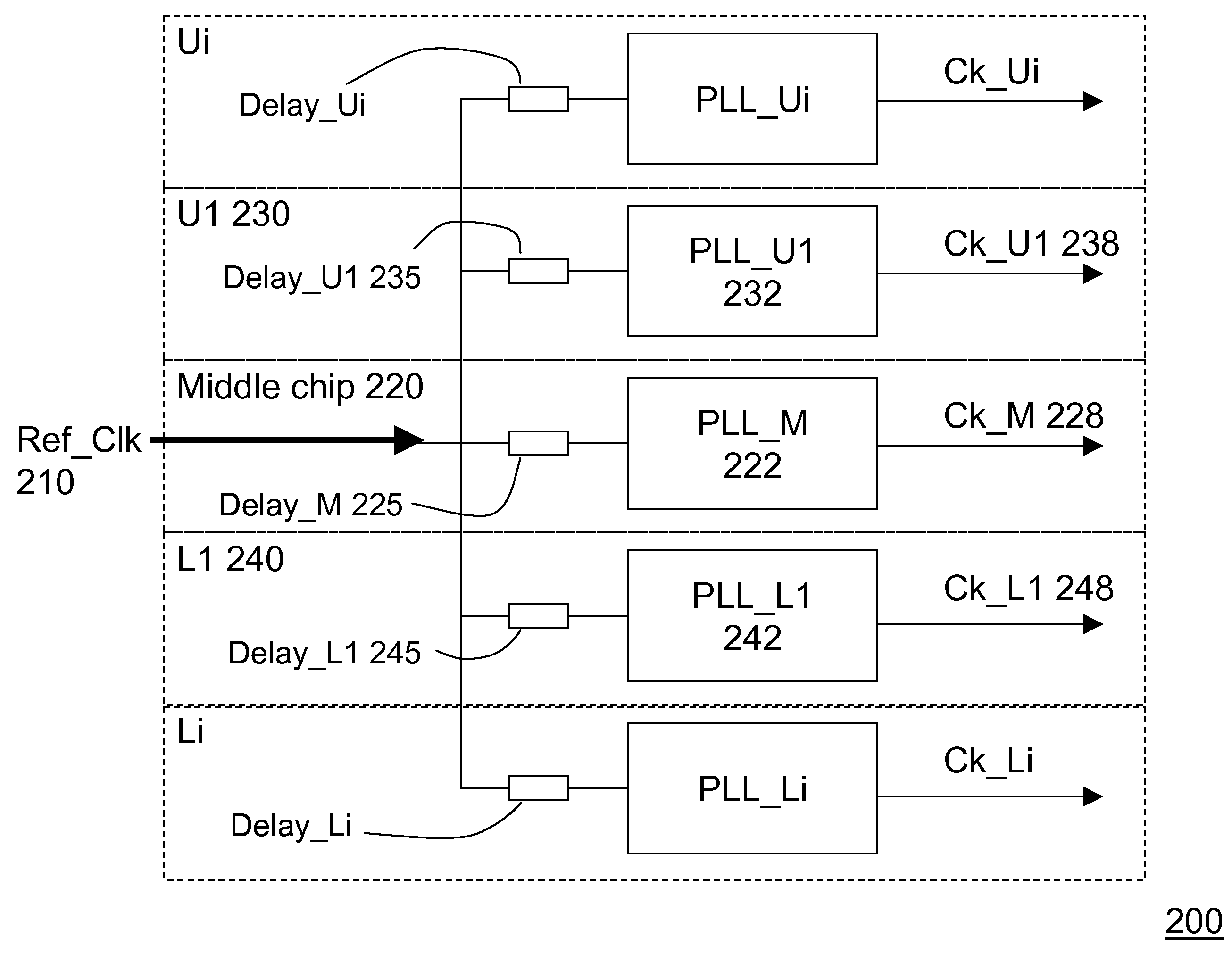
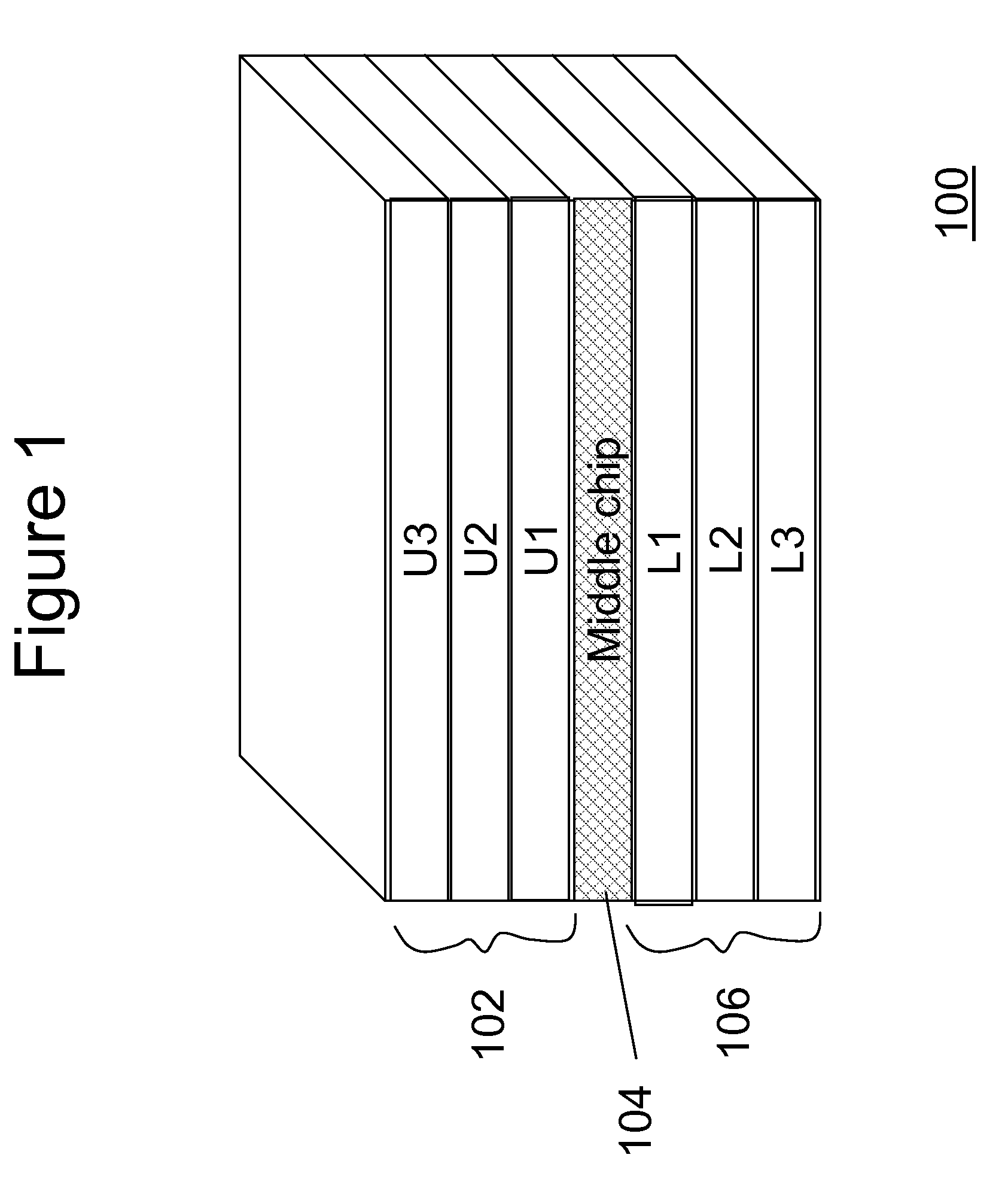
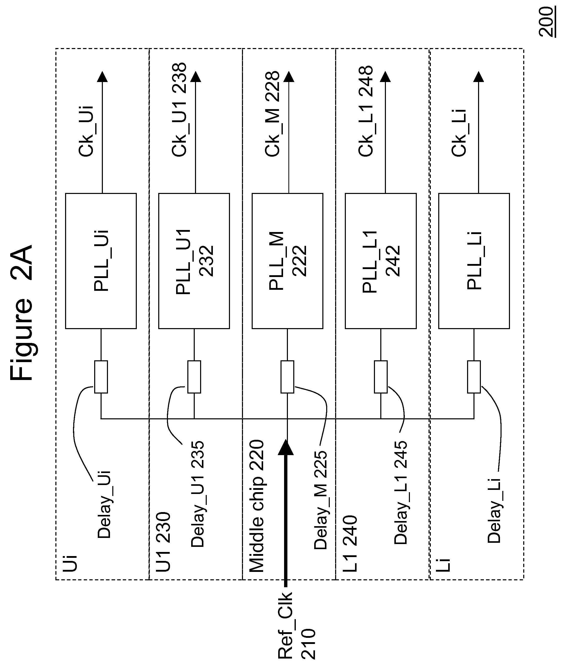
[0029]Referring to FIG. 1, there is shown an embodiment of a stacked chip structure 100. Although seven chips are shown, it is to be understood that other number of chips may be stacked to form the chip stack. In this example, a central reference clock is preferably placed in a middle chip 104 and a plurality of reference clock signals are routed to three upper chips 102 (U1, U2 and U3) (“child chip”) and three lower chips 106 (L1, L2 and L3) (“child chip”).
[0030]In general, such chips may be fabricated at the wafer level with standard devices and circuits formed in layers of the front-end of line (FEOL). Interconnects and dielectrics are then formed in layers of back-end of line (BEOL). All the chips are ...
PUM
 Abstract
Description
Claims
Application Information


