Driving method for a liquid crystal display

a liquid crystal display and driving method technology, applied in static indicating devices, instruments, cathode-ray tube indicators, etc., can solve the problems of large amount of motion images, induced rc delay effect, edge blur, etc., to reduce power consumption, avoid edge blur of images, and reduce power consumption. method

Active Publication Date: 2011-01-04
HANNSTAR DISPLAY CORPORATION
View PDF5 Cites 10 Cited by
  • Summary
  • Abstract
  • Description
  • Claims
  • Application Information

AI Technical Summary

Benefits of technology

[0022]Given the driving method according to an embodiment in the present invention, the voltage value of the pixel electrode is kept at a voltage value of the common electrode, or close to that. Therefore, edge blur of an image is avoided since black frame insertion and hold-type addressing method both applies to the LCD.
[0023]Given the driving method according to an embodiment of the present invention, an overdrive and reduced power consumption method is provided. The pixel electrode is pre-charged with a voltage value for overdrive the pixel so that power consumption is reduced according to this embodiment.
[0024]The method of this present invention, dot inversion driving applies for black frame insertion, liquid crystal overdrive, and reduced power consumption, so as to implement large dimensional LCD.
[0037]According to one aspect of the present invention, a LCD driving method is provided, wherein the pixel electrode is biased with a pre-charge voltage with capacitively coupled feedback method via storage capacitance to the neighboring scan line, so that difference between the voltage level of the pixel electrode and that of the common electrode is increase. When the voltage level of the pixel electrode is larger then that of the common electrode, the pixel electrode is biased with a positive pre-charge voltage when the voltage level thereof is smaller than that of the common electrode, and biased with a negative pre-charge voltage when the voltage level there of is larger than that of the common electrode, so that difference between the voltage level of the pixel electrode and that of the common electrode is increased.

Problems solved by technology

If serving the aforementioned conventional LCD as motion image display, e.g. current television system, a large amount of motion images is required.
Therefore edge blur is incurred.
On the other hand, RC delay effect is induced from gate circuitry, so that not applicable to panels with large dimension and higher resolution.
According to the conventional schemes mentioned above and technology that is known to the skill in the art, a lot of problems do exist, i.e. panels are not suitable for large dimension or high resolution, or only capable of row inversion driving method.
However, larger and larger dimension of LCD is required, where the driving method is thus developed as dot inversion driving method as opposed to conventional driving method that are outdated.

Method used


Image

  • Driving method for a liquid crystal display
  • Driving method for a liquid crystal display
  • Driving method for a liquid crystal display

Examples


first embodiment

The First Embodiment

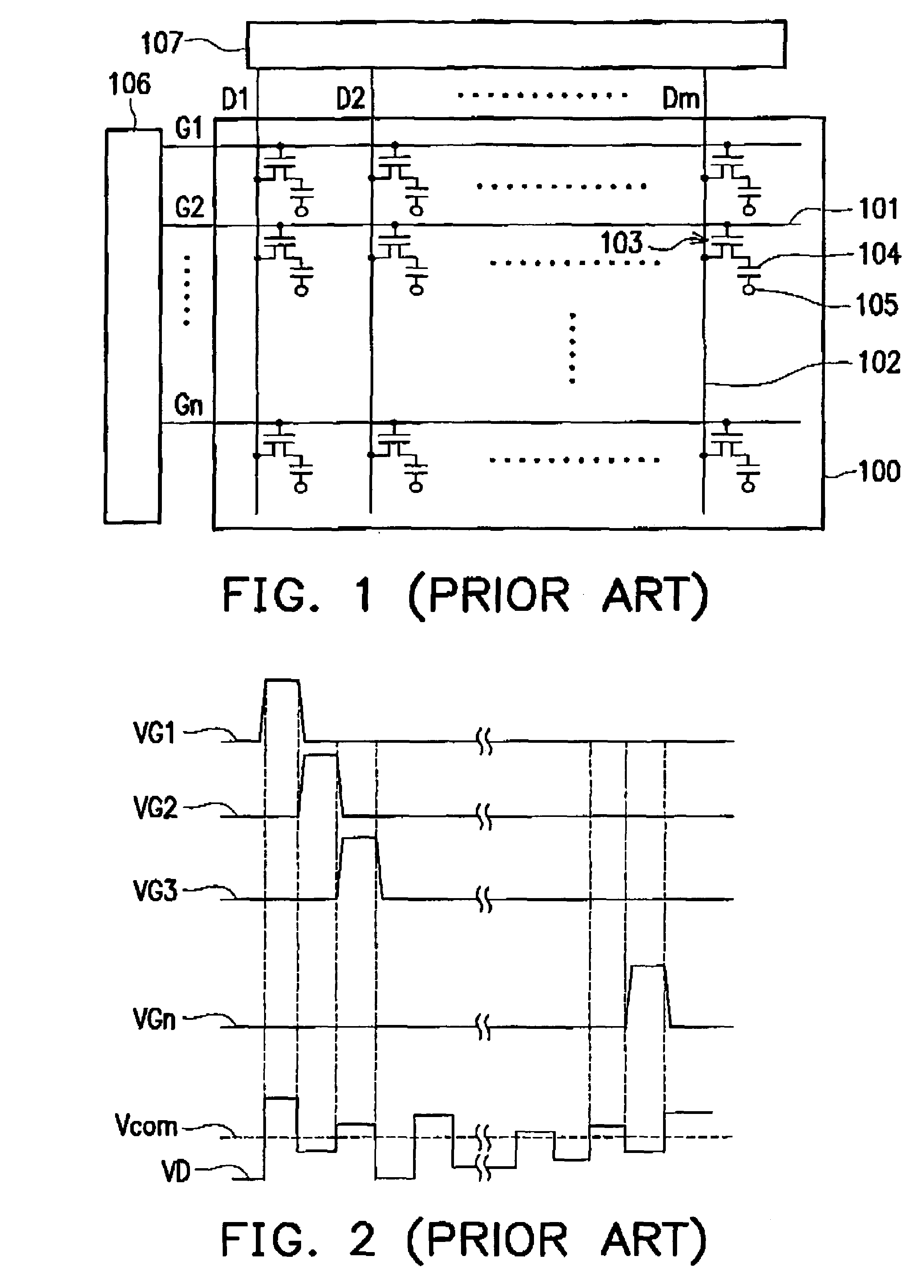
[0064]According to the first embodiment of the present invention, a driving method for a LCD is provided. Referring to FIG. 5, a LCD structure using the driving method according to one embodiment of the present invention is illustrated herein. The LCD structure includes scan lines G(n−1), G(n), and G(n+1), and signal lines D(m−1) and D(m). The corresponding pixels to the structured built with scan lines G(n−1), G(n), G(n+1) and signal lines D(m−1) and D(m) are pixel I, pixel II, pixel III, and pixel IV as illustrated in the figure.

[0065]Where a gate of the TFT of the pixel I is coupled to the scan line G(n−1), gates of the TFTs of the pixel II and III are coupled to the scan line G(n), and a gate of the TFT of the pixel IV is coupled to the scan line G(n+1). Sources of the TFTs of the pixel I and pixel III are coupled to the signal line D(m−1), and sources of the pixel II and pixel IV are coupled to the signal line D(m).

[0066]As illustrated in FIG. 5, for a same ...

second embodiment

The Second Embodiment

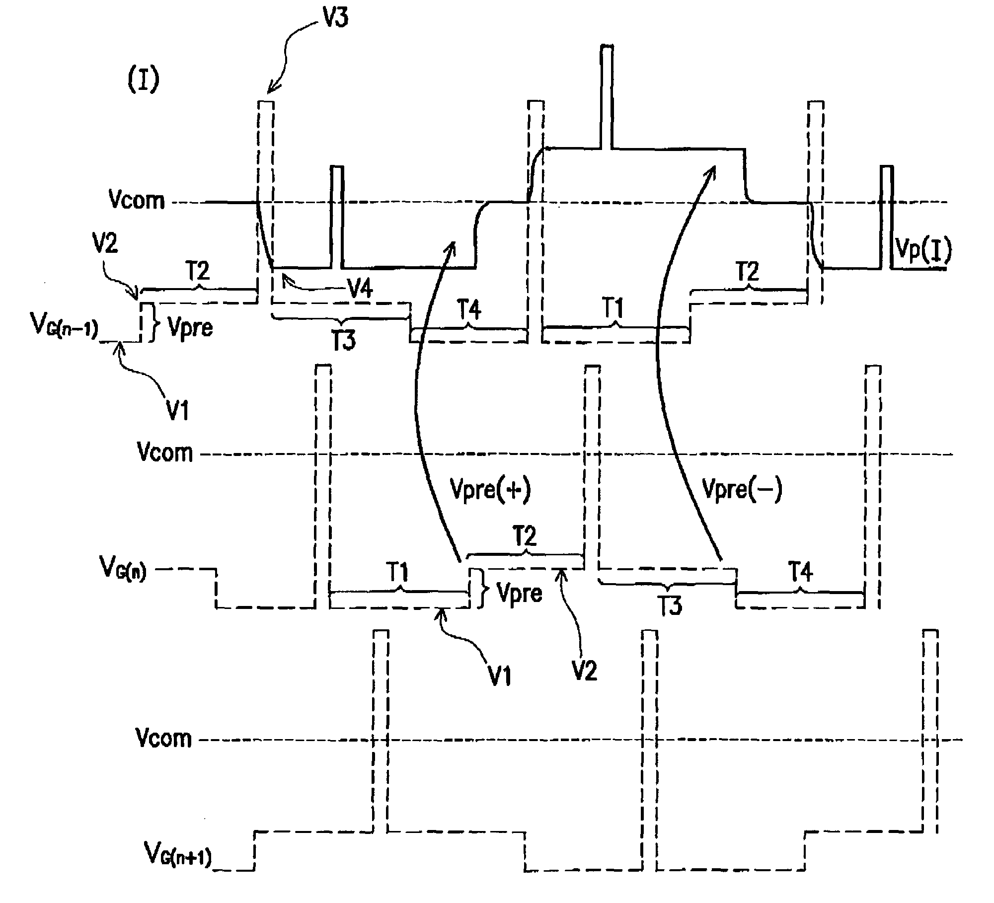
[0084]In another embodiment of the present invention, a scan line is pre-charged with a voltage Vpre for a feedback time interval T before a scan line of the LCD is biased with a scan signal, where voltage variation caused by the voltage Vpre does not manage to switch on the TFT thereof. The voltage Vpre is capacitively coupled to a pixel voltage of a previous or a next stage pixel that is coupled to the same scan line via a storage capacitor. For example, in the embodiment of the present invention along with description in FIG. 6, the voltage level of the pixel electrode is biased to or similar to that of the common electrode, i.e. Vcom.

[0085]Referring to FIG. 6, the LCD structure includes scan lines G(n−1), G(n), and G(n+1), and signal lines D(m−1) and D(m). The corresponding pixels to the structured built with scan lines G(n−1), G(n), G(n+1) and signal lines D(m−1) and D(m) are pixel I, pixel II, pixel III, and pixel IV as illustrated in the figure. Where a g...

third embodiment

The Third Embodiment

[0098]In another embodiment of the present invention, a driving method with liquid crystal overdrive and reduced power consumption is provided as illustrated in FIG. 7. Referring to FIG. 7, the LCD structure includes scan lines G(n−1), G(n), and G(n+1), and signal lines D(m−1) and D(m). The corresponding pixels to the structured built with scan lines G(n−1), G(n), G(n+1) and signal lines D(m−1) and D(m) are pixel I, pixel II, pixel III, and pixel IV as illustrated in the figure. Where a gate of the TFT of the pixel I is coupled to the scan line G(n−1), gates of the TFTs of the pixel II and III are coupled to the scan line G(n), and a gate of the TFT of the pixel IV is coupled to the scan line G(n+1). Sources of the TFTs of the pixel I and pixel III are coupled to the signal line D(m−1), and sources of the pixel II and pixel IV are coupled to the signal line D(m).

[0099]Referring to FIGS. 7A to 7D, schematic waveform diagrams of driving methods for pixel I, pixel I...


PUM

PropertyMeasurementUnit
transmittanceaaaaaaaaaa
voltageaaaaaaaaaa
pre-charge voltageaaaaaaaaaa

Abstract

A driving method for a liquid crystal display is provided. A pre-charge voltage value is applied to a scan line, where the voltage level does not manage to turn on the thin film transistor of the associated pixel, before a scan signal is applied to the scan line of the liquid crystal display. The pre-charge voltage level is electrically connected to the pixel voltage of the scan line via a storage capacitor to the neighboring pixel.

Description

CROSS-REFERENCE TO RELATED APPLICATION[0001]This application claims the priority benefit of Taiwan application serial no. 93109015, filed Apr. 1, 2004.BACKGROUND OF THE INVENTION[0002]1. Field of Invention[0003]The present invention relates to a driving method for a liquid crystal display, and more particularly, to a pre-charge method for a liquid crystal display, wherein a pre-charge voltage value is applied to a scan line before a scan signal is electrically coupled to the neighboring pixel via a storage capacitor.[0004]2. Description of the Related Art[0005]A liquid crystal display advances, not only in dimension thereof, but also in larger variety of image types. For example, most LCDs are used for still images on a personal computer or a word-processing product, yet currently most products are capable of displaying motion pictures, such as LCD television. Since a LCD is rather smaller and thinner than conventional cathode ray tube television, and is not space consuming after in...

Claims


Application Information

Patent Timeline
Patent Type & Authority Patents(United States)
IPC IPC(8): G09G3/36G09G3/18G02F1/133G09G3/20G09G5/00
CPCG09G3/3659G09G3/3614G09G2320/0252
Inventor SHIH, PO-SHENG
Owner HANNSTAR DISPLAY CORPORATION
Why Eureka
Try Eureka