Integrated circuit memory access mechanisms

a technology of access mechanism and integrated circuit, which is applied in the field can solve the problems of failure of integrated circuit memory, device that differs from its original design characteristics, and is more susceptible to manufacturing variation, so as to improve read robustness, increase read robustness, and improve read robustness

Inactive Publication Date: 2011-01-04
RGT UNIV OF MICHIGAN
View PDF5 Cites 0 Cited by
  • Summary
  • Abstract
  • Description
  • Claims
  • Application Information

AI Technical Summary

Benefits of technology

The present technique recognises that the first gate circuit and the second gate circuit which selectively couple the bit value retention circuit to respective nodes (such as bit lines) need not be controlled symmetrically such that during a write access both the first gate circuit and the second gate circuit may be opened whereas during a read access the first gate circuit may be opened and the second gate circuit may be closed. This asymmetric control of the first gate circuit and the second gate circuit permits a variety of design variations to be applied within the memory cell increasing its robustness of operation and yet not requiring a higher number of transistors.
The first gate circuit and the second gate circuit may comprise a first pass gate and a second pass gate with the first pass gate and the second pass gate having respective design parameters giving the first pass gate a lower conductance than the second pass gate. Giving the first pass gate a lower conductance and the second pass gate (i.e. making the first pass gate “weak”) has the result that the portions of the bit value retention circuit coupled to the first pass gate are less likely to be overwhelmed by an in-rush of charge when a read operation is performed resulting in a reduced likelihood of read upsets and more robust operation.
It will be appreciated that the nodes via which data access is made to the data retention circuit may be precharged so as to be discharged during a read or precharged so as to be charged during a read. When the nodes are to be selectively discharged via the second supply rail during a read operation, the first pull-down gate and the second pull-down gate can be formed to have respective design parameters giving the first pull-down gate a higher conductance than the second pull-down gate. Making the first pull-down gate “stronger” in this way increases the read robustness by reducing the likelihood that an in-rush of charge from the first node will overwhelm the first pull-down gate and result in a change in the bit value stored by the data retention circuit (a read upset).
In embodiments in which during a read access the first node is selectively charged via the first supply rail, the first pull-up gate and the second pull-up gate can be formed to have respective design parameters giving the first pull-up gate a higher conductance than the second pull-up gate. Forming a “strong” first pull-up gate in this way similarly increases read robustness by resisting the likelihood of an out-rush of charge from the data retention circuit to the first node overwhelming the first pull-up gate and changing the data value stored.
In the context of a memory cell in which the first pass gate has been formed so as to be weaker than the second pass gate (e.g. to improve read robustness), during a write access that forces a change in signal level of the output of the first inverter away from a signal level of the first supply rail, the first pull-up gate will act to oppose this change. Given that the first pass gate is weak, the likelihood of the first pull-up gate being too strong to permit a write (and thereby causing a write error) can be reduced by forming the memory circuit such that the first pull-up gate and the second pull-up gate have respective design parameters giving the first pull-up gate a lower conductance than the second pull-up gate. Forming the first pull-up gate with a lower conductance (i.e. “weak”) has the result that the weak first pass gate is still able to force a change of state necessary for a write operation.
In alternative embodiments it may be that during a write access that forces a change in signal level of the output of the first inverter away from the signal level of the second supply rail, the first pull-down gate will act to oppose this change. In this context the first pull-down gate and the second pull-down gate can be formed to have respective design parameters giving the first pull-down gate a lower conductance than the second pull-down gate. Thus, forming a “weak” first pull-down gate in this way reduces the likelihood that the “weak” first-pass gate will be unable to force a write.

Problems solved by technology

However, a problem with the use of smaller devices is that they are more susceptible to manufacturing variation whereby imperfect manufacture causes a device to differ from its original design characteristics.
This variation may result in the device failing to operate as intended and causing a failure within the integrated circuit memory.
This reduces the manufacturing yield which may be achieved and makes the integrated circuit memories more expensive.
Examples of failures which can arise within integrate circuit memories include failures in write and / or read operations to individual data retention circuits (memory cells).
A lack of robustness in write and read operations is becoming a significant problem in the production of high density, low power and low cost integrated circuit memories.
However, a problem with the 6T memory cell at small device geometries is that variation in the characteristics of the individual devices (transistors / gates) can result in incorrect read operation and / or incorrect write operation.
Forcing such a change of state of the data retention circuit 2 would be difficult if the pass gates 12, 14 were made insufficiently conductive, thereby impacting the write robustness.
This reduces the memory cell density which can be achieved as well as increasing the power consumption and cost of the integrated circuit memory.
These further known memory cell designs also both suffer from the disadvantage of requiring a higher number of dates per sell and the same disadvantages as discussed above in relation to FIG. 1.

Method used


Image

  • Integrated circuit memory access mechanisms
  • Integrated circuit memory access mechanisms
  • Integrated circuit memory access mechanisms

Examples


Embodiment Construction

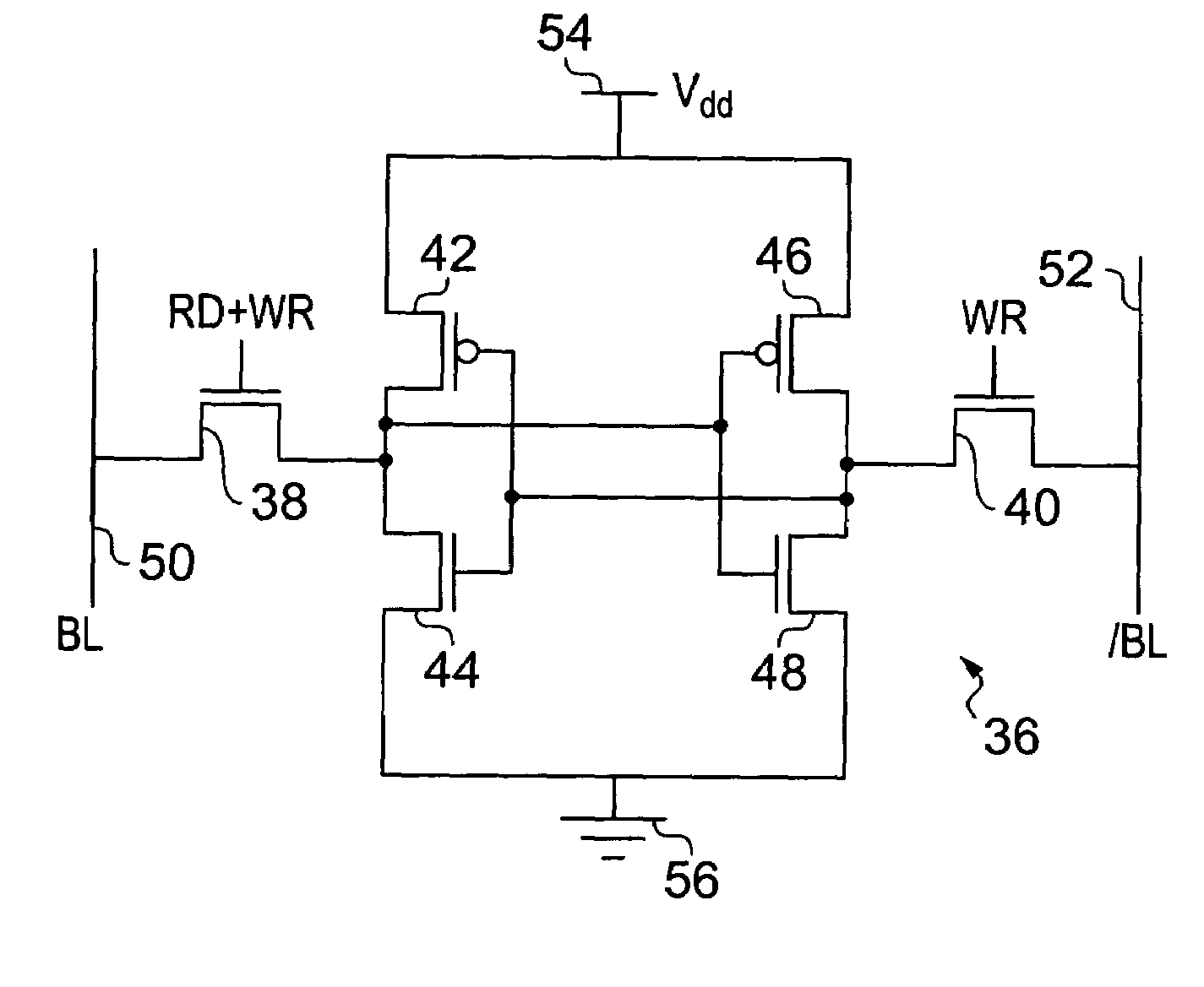
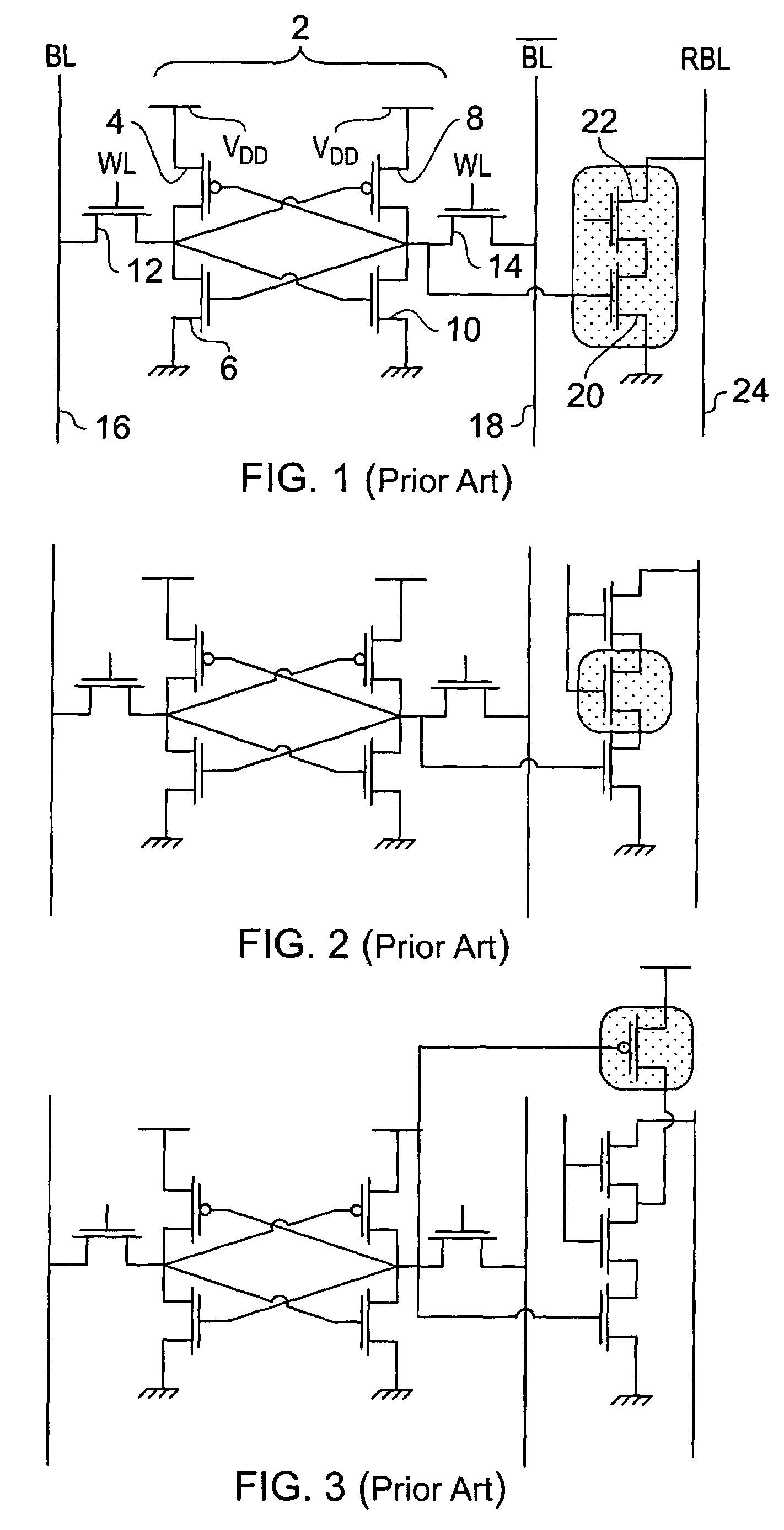
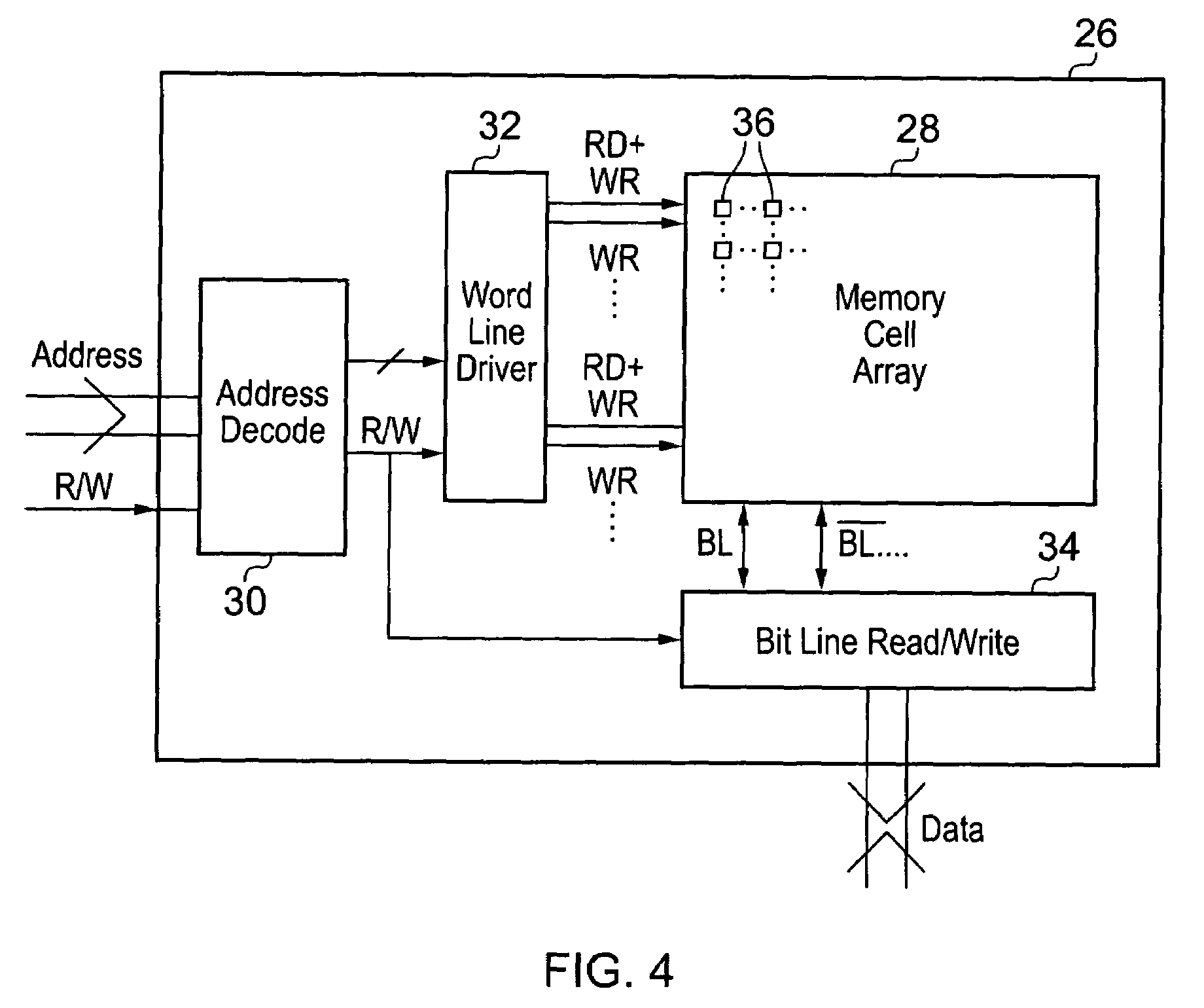
FIG. 4 shows an integrated circuit memory 26 including a memory cell array 28, an address decoder 30, a word line driver 32 and a bit line read / write circuit 34. It will be appreciated that the integrated circuit memory 26 will typically include many other circuit elements, but these have been omitted from FIG. 4 for the sake of clarity. It will also be appreciated that the integrated circuit memory 26 may be formed as a discrete package on its own or as part of an integrated circuit which contains other circuit elements, such as a processor core, cache memory, DSP circuit etc (as typically used in system-on-chip integrated circuits).

In operation the integrated circuit memory 26 receives an address to be accessed and a signal indicating whether a read operation or a write operation is to be performed. The address decoder 30 responds to this received address to pass appropriate control signals to the word line driver 32 (which may be considered to be an access controller either on it...


PUM


Abstract

A memory cell 36 within an integrated circuit memory is provided with an access controller 32 coupled to a first pass gate 38 and a second pass gate 40. During a write access to the memory cell 38 both the first pass gate 38 and the second pass gate 40 are opened. During a read access, the first pass gate 38 is opened and the second pass gate 40 is closed. This asymmetry in the read and write operations permits an asymmetry in the gates forming the memory cell 36 thereby permitting changes to increase both read robustness and write robustness. The asymmetry in the design parameters of different gates can take the form of varying the gate length, the gate width and the threshold voltage so as to vary the conductance of different gates to suit their individual role within the memory cell 36 which is operating in the asymmetric manner provided by the separate word line signals driving read operations and write operations.

Description

BACKGROUND OF THE INVENTION1. Field of the InventionThis invention relates to the field of integrated circuit memories. More particularly, this invention relates to access mechanisms used for reading and writing data values within integrated circuit memories.2. Description of the Prior ArtIt is desirable within the field of integrated circuit memories that the storage density should be high thereby enabling large quantities of data to be stored. Furthermore, it is desirable that the power consumption of the integrated circuit memories should be low and their cost should be low. In order to help meet these requirements there has been a steady trend to the use of smaller device geometries. These smaller devices, such as devices based upon 45 nm manufacturing techniques, enable higher density memories to be achieved with lower power consumption. However, a problem with the use of smaller devices is that they are more susceptible to manufacturing variation whereby imperfect manufacture ...

Claims


Application Information

Patent Timeline
Patent Type & Authority Patents(United States)
IPC IPC(8): G11C11/40
CPCG11C11/419
Inventor CHEN, GREGORY KENGHOSYLVESTER, DENNIS MICHAELBLAAUW, DAVID THEODORE
Owner RGT UNIV OF MICHIGAN
Why Eureka
Try Eureka