Nitride semiconductor light emitting device including electrodes of a multilayer structure

a multi-layer structure, light-emitting device technology, applied in the direction of semiconductor devices, basic electric elements, electrical appliances, etc., can solve the problems of reducing the entire luminous efficiency of the device, reducing the light extraction efficiency, and difficult to form ohmic contact with the electrode, so as to improve reliability, excellent reflectivity and reduce the heating value of the device.

Active Publication Date: 2011-01-11
SAMSUNG ELECTRONICS CO LTD
View PDF11 Cites 6 Cited by
  • Summary
  • Abstract
  • Description
  • Claims
  • Application Information

AI Technical Summary

Benefits of technology

[0020]An advantage of the present invention is that it provides a nitride semiconductor LED in which an n-electrode and p-electrode, having low ohmic contact resistance and having a multilayer structure formed of a material with excellent reflectivity and heat resistance, respectively are provided on n-type and p-type nitride semiconductor layers. Therefore, the heating value of the device can be reduced to improve reliability. Further, some light emitted from an active layer can be prevented from being absorbed into the n-electrode and p-electrode, thereby enhancing the light extraction efficiency.
[0021]Additional aspects and advantages of the present general inventive concept will be set forth in part in the description which follows and, in part, will be obvious from the description, or may be learned by practice of the general inventive concept.
[0022]According to an aspect of the invention, a nitride semiconductor LED comprises a substrate; an n-type nitride semiconductor layer formed on the substrate; an active layer formed on a predetermined region of the n-type nitride semiconductor layer; a p-type nitride semiconductor layer formed on the active layer; a p-electrode formed on the p-type nitride semiconductor layer; and an n-electrode formed on the n-type nitride semiconductor layer in which the active layer is not formed. The p-electrode and n-electrode are formed to have such a multilayer structure that an ohmic contact layer, a compound layer containing aluminum or silver, and a degradation preventing layer are sequentially laminated.
[0023]According to another aspect of the invention, the nitride semiconductor LED further comprises a current spreading layer formed at the interface between the p-type nitride semiconductor layer and the p-electrode.
[0024]According to a further aspect of the invention, a nitride semiconductor LED comprises an n-electrode; an n-type nitride semiconductor layer formed under the n-electrode; an active layer formed under the n-type nitride semiconductor layer; a p-type nitride semiconductor layer formed under the active layer; a p-electrode formed under the p-type nitride semiconductor layer; and a support layer formed under the p-electrode. The p-electrode and n-electrode are formed to have such a multilayer structure that an ohmic contact layer, a compound layer containing aluminum or silver, and a degradation preventing layer are sequentially laminated from the surface of the adjacent nitride semiconductor layer.
[0025]According to a still further aspect of the invention, the ohmic contact layer is formed of Cr or a compound layer containing Cr. The ohmic contact layer improve ohmic contact resistance of the n-type and p-type nitride semiconductor layers having a relatively large energy band gap and to enhance an adhesive force between the n-type and p-type nitride semiconductor layers and the compound layer containing aluminum or silver.

Problems solved by technology

However, since such a nitride semiconductor has a relatively large energy band-gap, it is difficult to form the ohmic contact with an electrode.
Therefore, light emitted from an active layer is not totally reflected, but is partially absorbed, thereby reducing the light extraction efficiency.
However, the p-electrode and n-electrode absorbs some light emitted from the active layer, thereby reducing the entire luminous efficiency of the device.
Further, since the p-electrode 160 and the n-electrode 170 are formed of Cr / Au, some light emitted from the active is absorbed, thereby reducing the entire luminous efficiency of the device.

Method used


Image

  • Nitride semiconductor light emitting device including electrodes of a multilayer structure
  • Nitride semiconductor light emitting device including electrodes of a multilayer structure
  • Nitride semiconductor light emitting device including electrodes of a multilayer structure

Examples


first embodiment

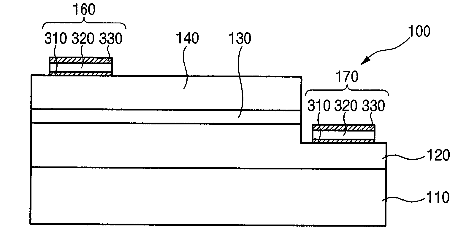
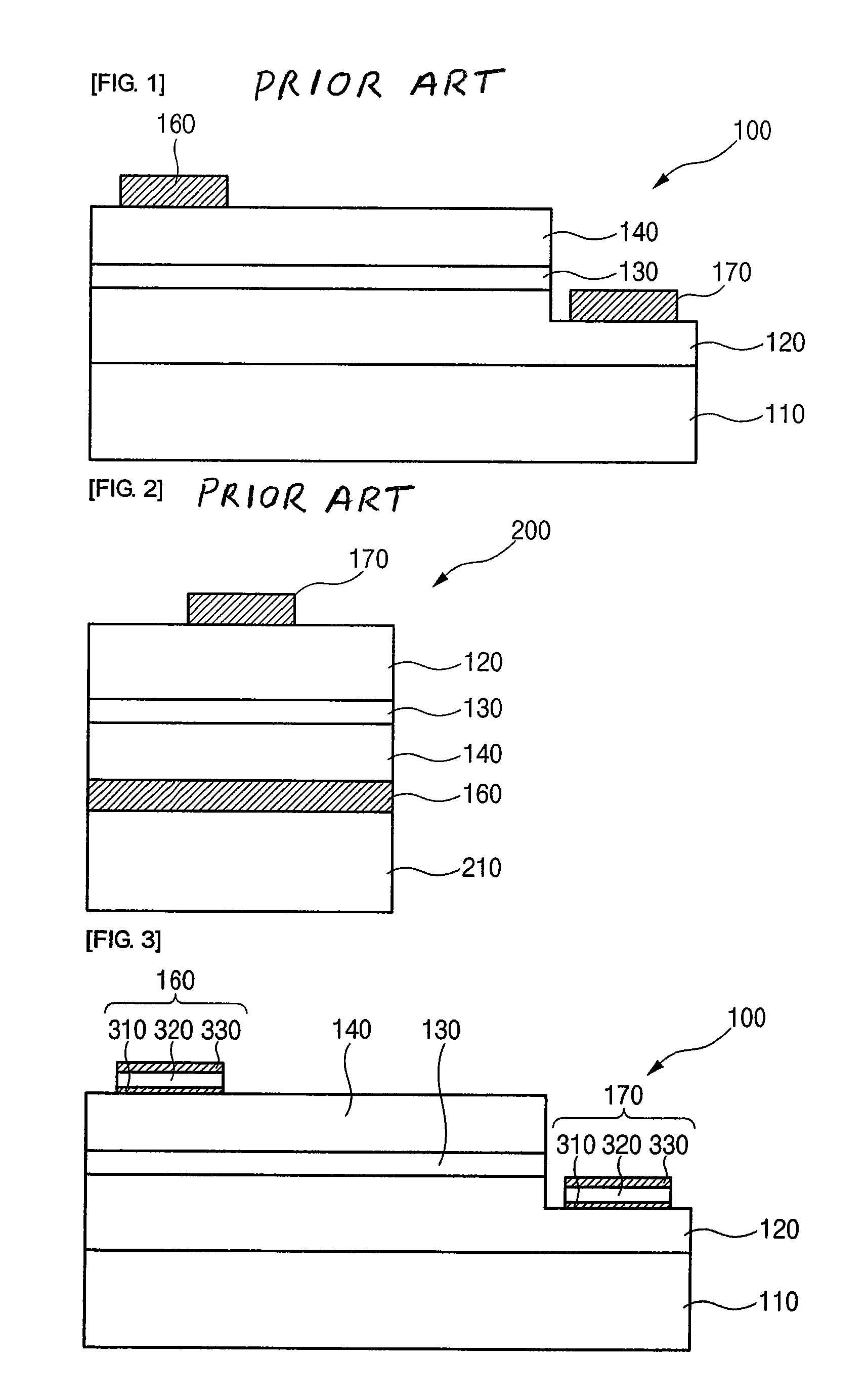
[0039]First, a nitride semiconductor LED according to a first embodiment of the invention will be described in detail with reference to FIG. 3. FIG. 3 is a sectional view illustrating the structure of the nitride semiconductor LED according to the first embodiment of the invention.

[0040]As shown in FIG. 3, a buffer layer (not shown), an n-type nitride semiconductor layer 120, an active layer 130, and a p-type nitride semiconductor layer 140 are sequentially formed on a substrate 110.

[0041]Preferably, the substrate 110 is formed of a transparent material including sapphire. Except for sapphire, the substrate 110 may be formed of zinc oxide (ZnO), gallium nitride (GaN), silicon carbide (SiC), or aluminum nitride (AlN).

[0042]The buffer layer (not shown) is formed of GaN and may be omitted.

[0043]The n-type or p-type nitride semiconductor layer 120 or 140 is formed of a GaN layer or GaN / AlGaN layer doped with conductive impurities, and the active layer 130 is formed to have a multi-quant...

second embodiment

[0060]Referring to FIG. 6, a second embodiment of the invention will be described. The descriptions of the same parts as the first embodiment of the present invention will be omitted for conciseness.

[0061]FIG. 6 is a sectional view illustrating the structure of a nitride semiconductor LED according to the second embodiment of the invention.

[0062]The nitride semiconductor LED 200 according to the second embodiment has almost the same construction as the nitride semiconductor LED according to the first embodiment. As shown in FIG. 6, however, the n-electrode 170 is formed on the rear surface of the n-type nitride semiconductor layer 120 on which the active layer 130 is formed, compared with the first embodiment in which the n-electrode 170 having a multilayer structure is formed on the n-type nitride semiconductor layer 120 exposed by removing portions of the active layer 130 and the p-type nitride semiconductor layer 140. Further, a support layer 210 is bonded to the rear surface of ...


PUM


Abstract

A nitride semiconductor LED comprises a substrate; an n-type nitride semiconductor layer formed on the substrate; an active layer formed on a predetermined region of the n-type nitride semiconductor layer; a p-type nitride semiconductor layer formed on the active layer; a p-electrode formed on the p-type nitride semiconductor layer; and an n-electrode formed on the n-type nitride semiconductor layer in which the active layer is not formed. The p-electrode and n-electrode are formed to have such a multilayer structure that an ohmic contact layer, a compound layer containing aluminum or silver, and a degradation preventing layer are sequentially laminated.

Description

CROSS-REFERENCE TO RELATED APPLICATIONS[0001]The application claims the benefit of Korea Patent Application No. 2005-84006 filed with the Korea Intellectual Property Office on Sep. 9, 2005, the disclosure of which is incorporated herein by reference.BACKGROUND OF THE INVENTION[0002]1. Field of the Invention[0003]The present invention relates to a nitride semiconductor light emitting diode (LED) which maintains low ohmic contact resistance, thereby enhancing the light extraction efficiency.[0004]2. Description of the Related Art[0005]In general, a nitride semiconductor is such a material that has a relatively high energy band gap (in the case of GaN semiconductor, about 3.4 eV), and is positively adopted in an optical device for generating green or blue short-wavelength light. As such a nitride semiconductor, a material having a composition of AlxInyGa1-x-y)N (herein, 0≦x≦1, 0≦y≦1, and 0≦x+y≦1) is widely used.[0006]However, since such a nitride semiconductor has a relatively large en...

Claims


Application Information

Patent Timeline
Patent Type & Authority Patents(United States)
IPC IPC(8): H01L33/00H01L33/10H01L33/14H01L33/32H01L33/40
CPCH01L33/405H01L33/32H01L2933/0016
Inventor KANG, PIL GEUNYI, BONG ILHAN, JAE HOJEON, DONG MIN
Owner SAMSUNG ELECTRONICS CO LTD
Why Eureka
Try Eureka