Semiconductor integrated circuit device
a technology of integrated circuits and semiconductors, applied in semiconductor devices, basic electric elements, instruments, etc., can solve the problems of large current requirements, large memory capacity of nonvolatile memories, and inability to multi-layered wiring, etc., to achieve accurate supply, less voltage drop, and higher reliability
- Summary
- Abstract
- Description
- Claims
- Application Information
AI Technical Summary
Benefits of technology
Problems solved by technology
Method used
Image
Examples
first embodiment
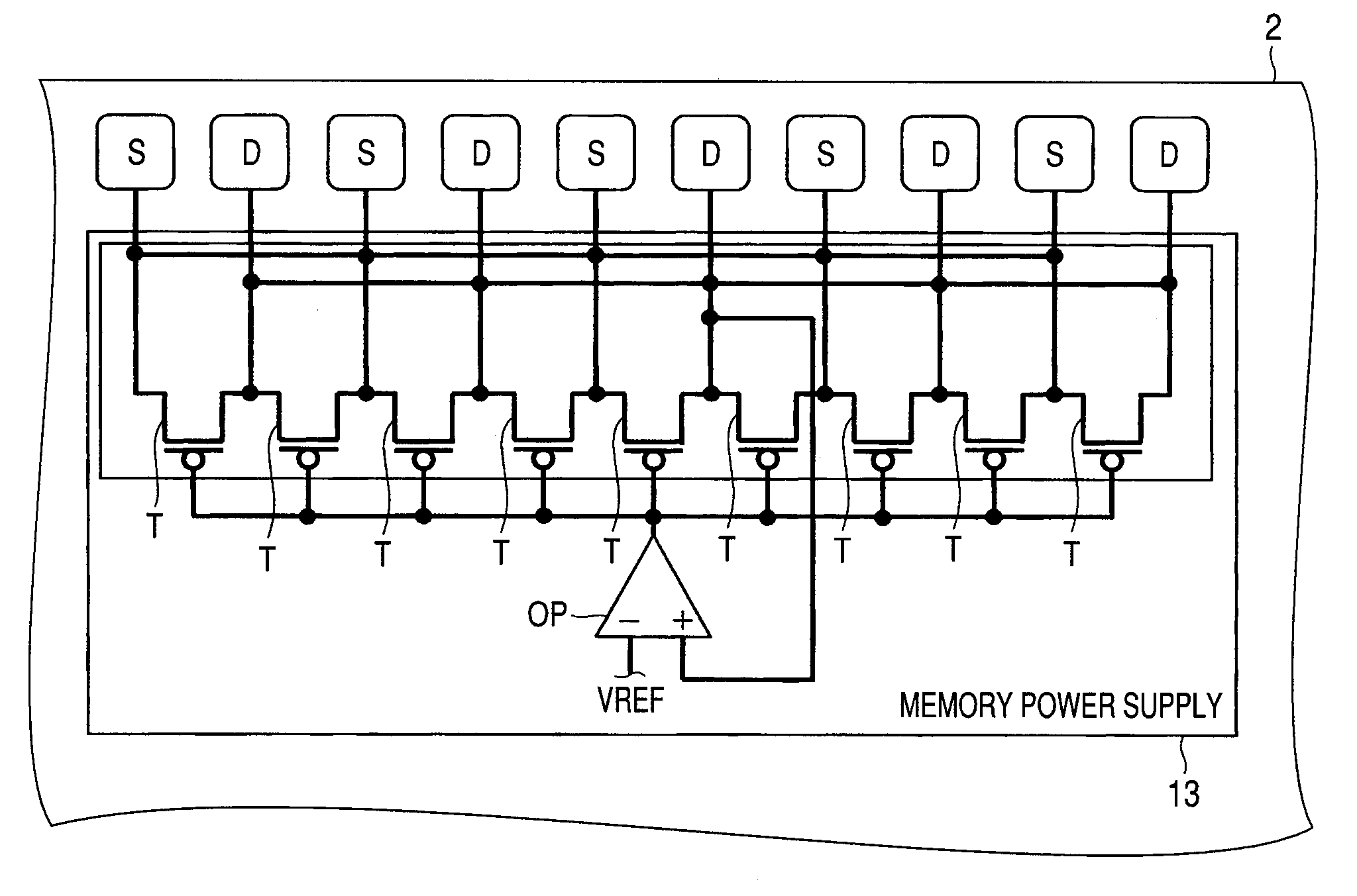
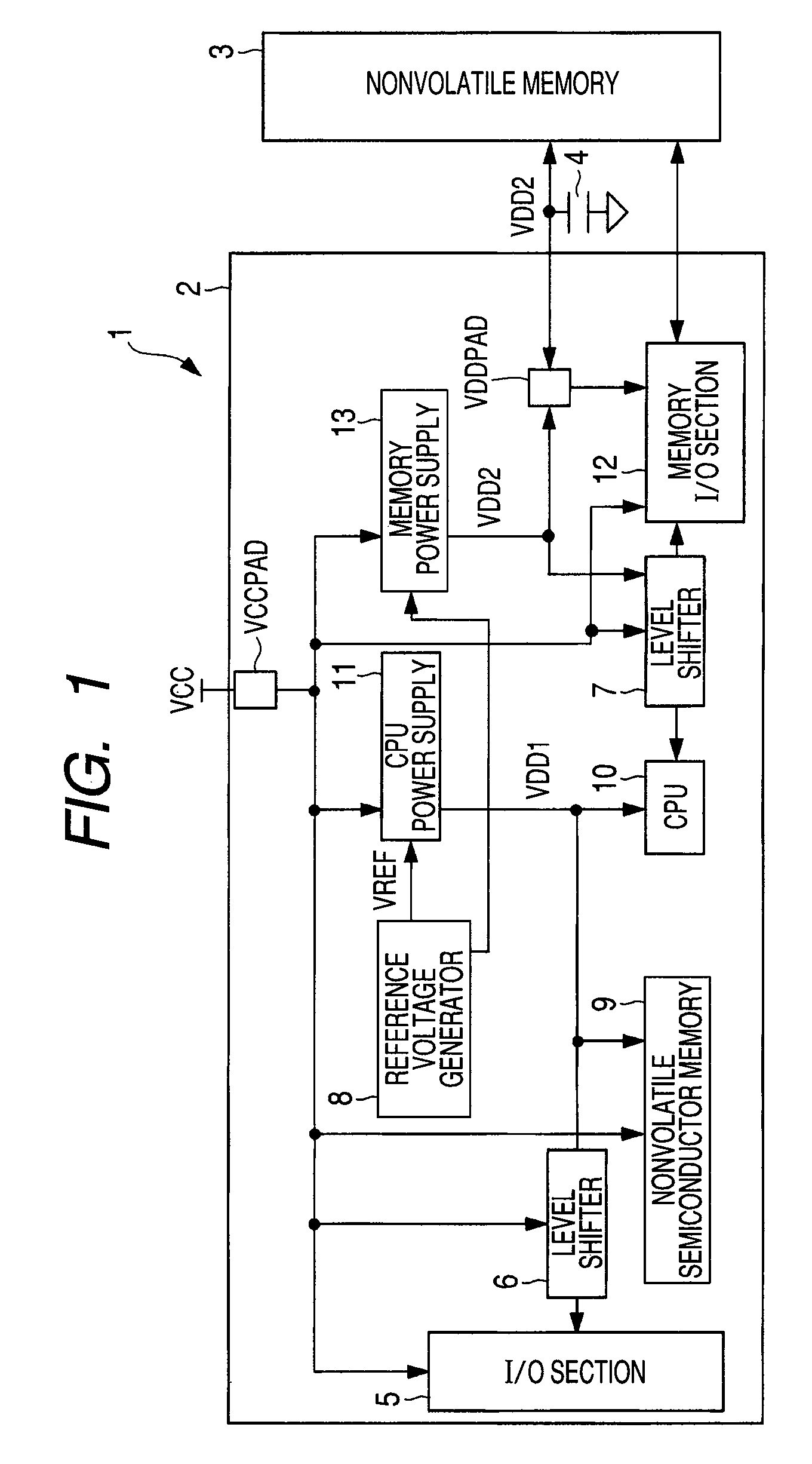
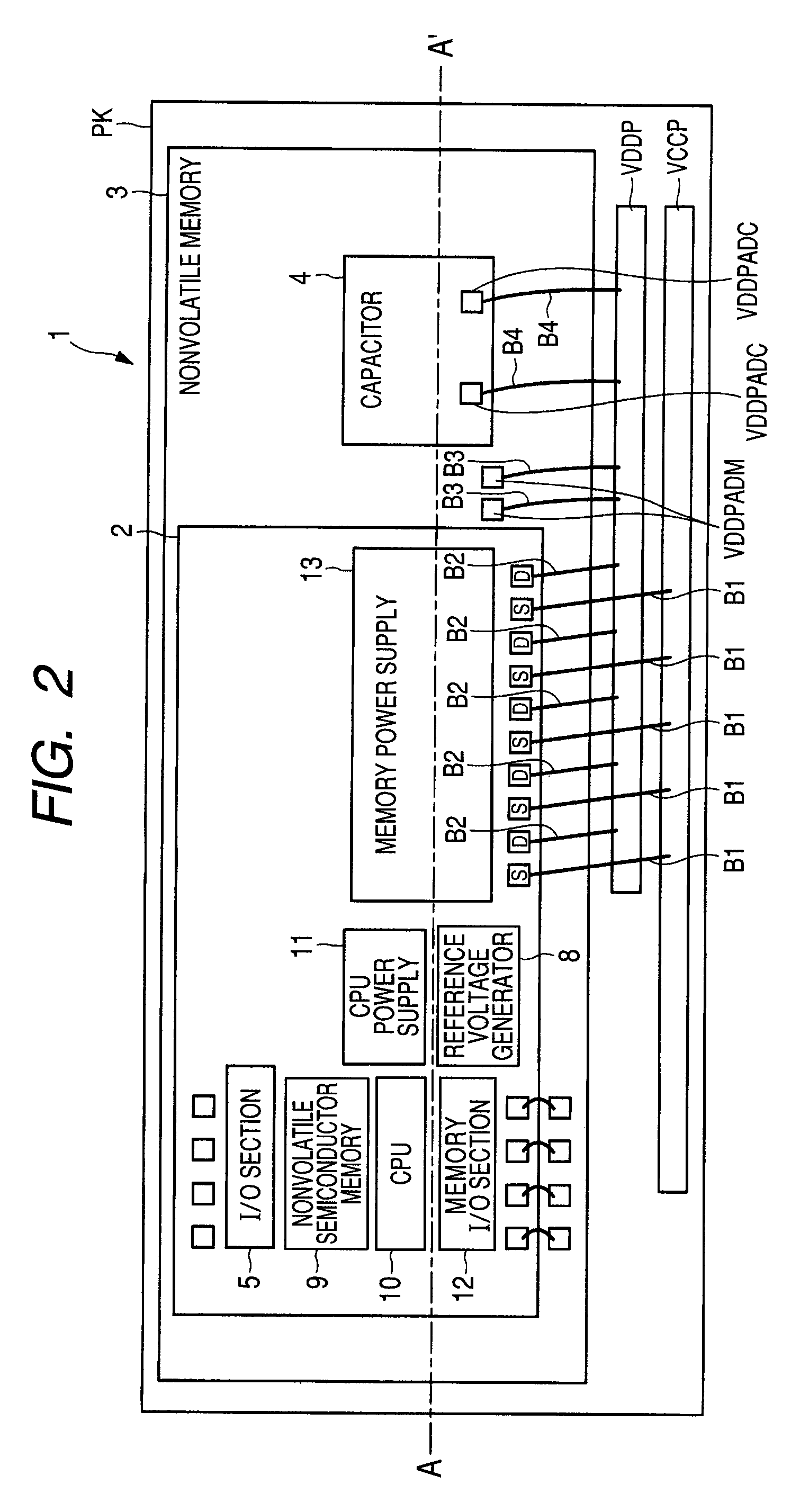
[0046]FIG. 1 is a block diagram showing the configuration of a semiconductor integrated circuit device according to a first embodiment of the present invention; FIG. 2 illustrates an example of package layout of the semiconductor integrated circuit device shown in FIG. 1; FIG. 3 is a sectional view taken along A-A′ in FIG. 2; FIG. 4 shows an example of the arrangement and connection pattern of source pads and drain pads in a memory power supply of the semiconductor integrated circuit device in FIG. 1; FIG. 5 illustrates an example of the layout pattern of the transistors in the memory power supply shown in FIG. 4; FIG. 6 is a sectional view taken along the line A-A′ in FIG. 5; FIG. 7 is a sectional view taken along the line B-B′ in FIG. 5; FIG. 8 illustrates an example of the arrangement of drain wirings and source wirings in the memory power supply in FIG. 4; and FIG. 9 illustrates the arrangement of drain wirings and source wirings in the memory power supply which the inventors ha...
second embodiment
[0091]FIG. 10 illustrates an example of package layout of a semiconductor integrated circuit device according to a second embodiment of the present invention and FIG. 11 is a sectional view taken along the line A-A′ in FIG. 10.
[0092]As in the foregoing first embodiment (FIG. 1), a semiconductor integrated circuit device 1 in the second embodiment includes a microcomputer 2, a nonvolatile memory 3, and a capacitor 4. The microcomputer 2 and the nonvolatile memory 3 are each formed on a single semiconductor chip.
[0093]The difference from the first embodiment is the package layout of the semiconductor integrated circuit device 1.
[0094]FIG. 10 illustrates an example of package layout of a semiconductor integrated circuit device according to the second embodiment of the present invention and FIG. 11 is a sectional view taken along the line A-A′ in FIG. 10.
[0095]As shown in FIG. 10, the nonvolatile memory 3 semiconductor chip lies in an upper part of a package substrate PK, and the microc...
third embodiment
[0105]FIG. 12 illustrates an example of the arrangement and connection pattern of source pads S and drain pads D in the memory power supply according to a third embodiment of the present invention; FIG. 13 illustrates an example of the layout pattern of transistors T in the memory power supply shown in FIG. 12; FIG. 14 is a sectional view taken along the line A-A′ in FIG. 13; and FIG. 15 is a sectional view taken along the line B-B′ in FIG. 13.
[0106]In the third embodiment, the semiconductor integrated circuit device 1 includes a microcomputer 2, a nonvolatile memory 3 and a capacitor 4 as in the first embodiment (FIG. 1). The microcomputer 2 and the nonvolatile memory 3 are each formed on a single semiconductor chip.
[0107]In the third embodiment, pads of the same type are grouped together unlike the first embodiment in which the drain pads D and source pads S in the memory power supply 13 are alternately arranged.
[0108]FIG. 12 illustrates an example of the arrangement and connectio...
PUM
 Abstract
Description
Claims
Application Information


