Electro-optical device, driving method of electro-optical device and electronic apparatus

a driving method and electrooptical technology, applied in the direction of instruments, static indicating devices, etc., can solve the problems of difficult to output data signals with extremely fine precision, display non-uniformity, etc., and achieve the effect of high precision and fine precision

Active Publication Date: 2013-04-18
SEIKO EPSON CORP
View PDF4 Cites 22 Cited by
  • Summary
  • Abstract
  • Description
  • Claims
  • Application Information

AI Technical Summary

Benefits of technology

[0008]An advantage of some aspects of the invention is that it provides an electro-optical device, a driving method of an electro-optical device and an electronic apparatus capable of supplying the current supplied to a light emitting element with high precision while compensating for the characteristics of the transistor without a need for a data signal with fine precision.

Problems solved by technology

At this time, when the characteristics such as the threshold voltage of the transistor are varied in each pixel circuit, display nonuniformity impairing the uniformity of the display screen is generated.
In a circuit having a high driving capability in this manner, it is difficult to output the data signal with extremely fine precision.

Method used


Image

  • Electro-optical device, driving method of electro-optical device and electronic apparatus
  • Electro-optical device, driving method of electro-optical device and electronic apparatus
  • Electro-optical device, driving method of electro-optical device and electronic apparatus

Examples


first embodiment

Operation of First Embodiment

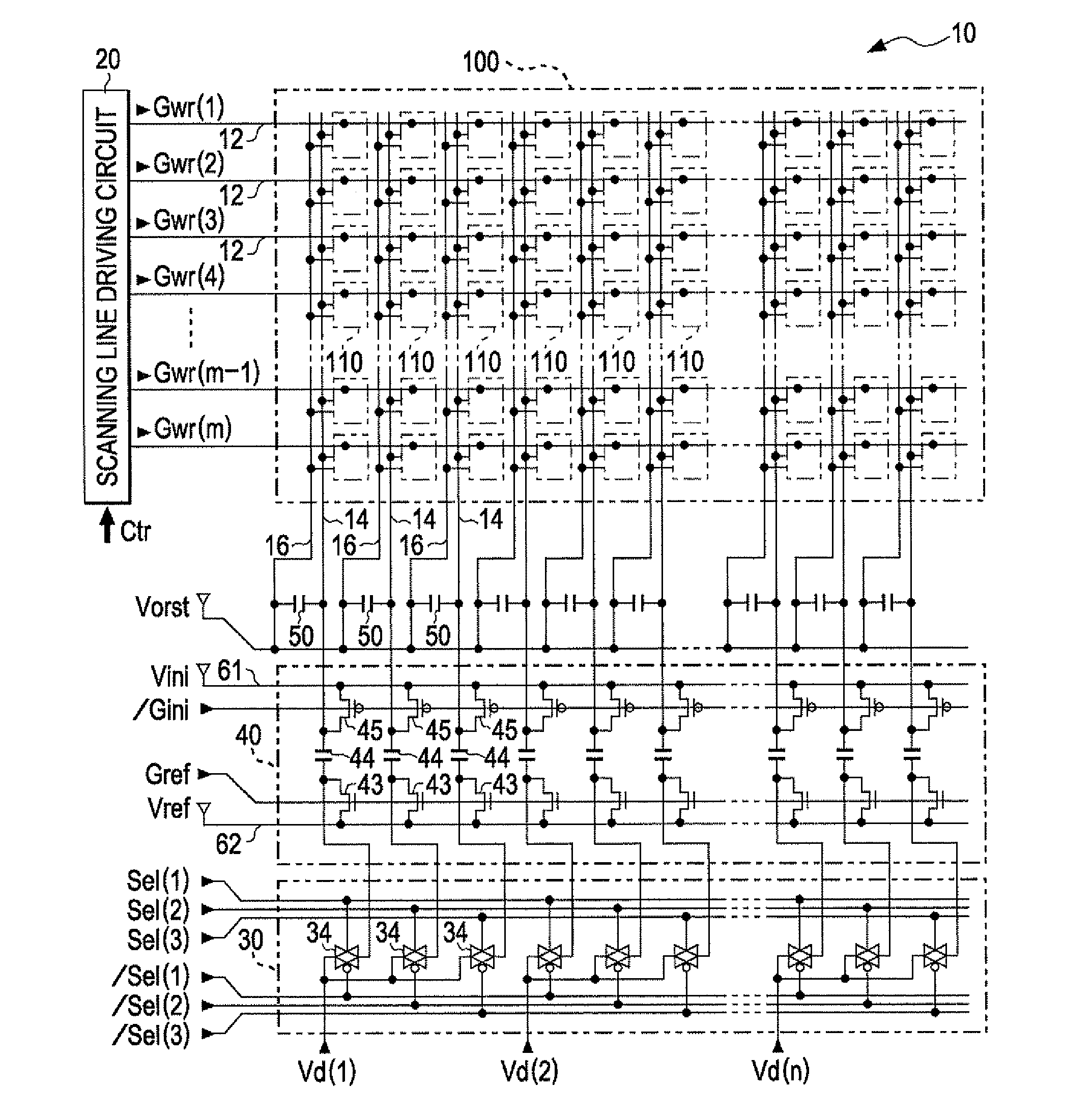
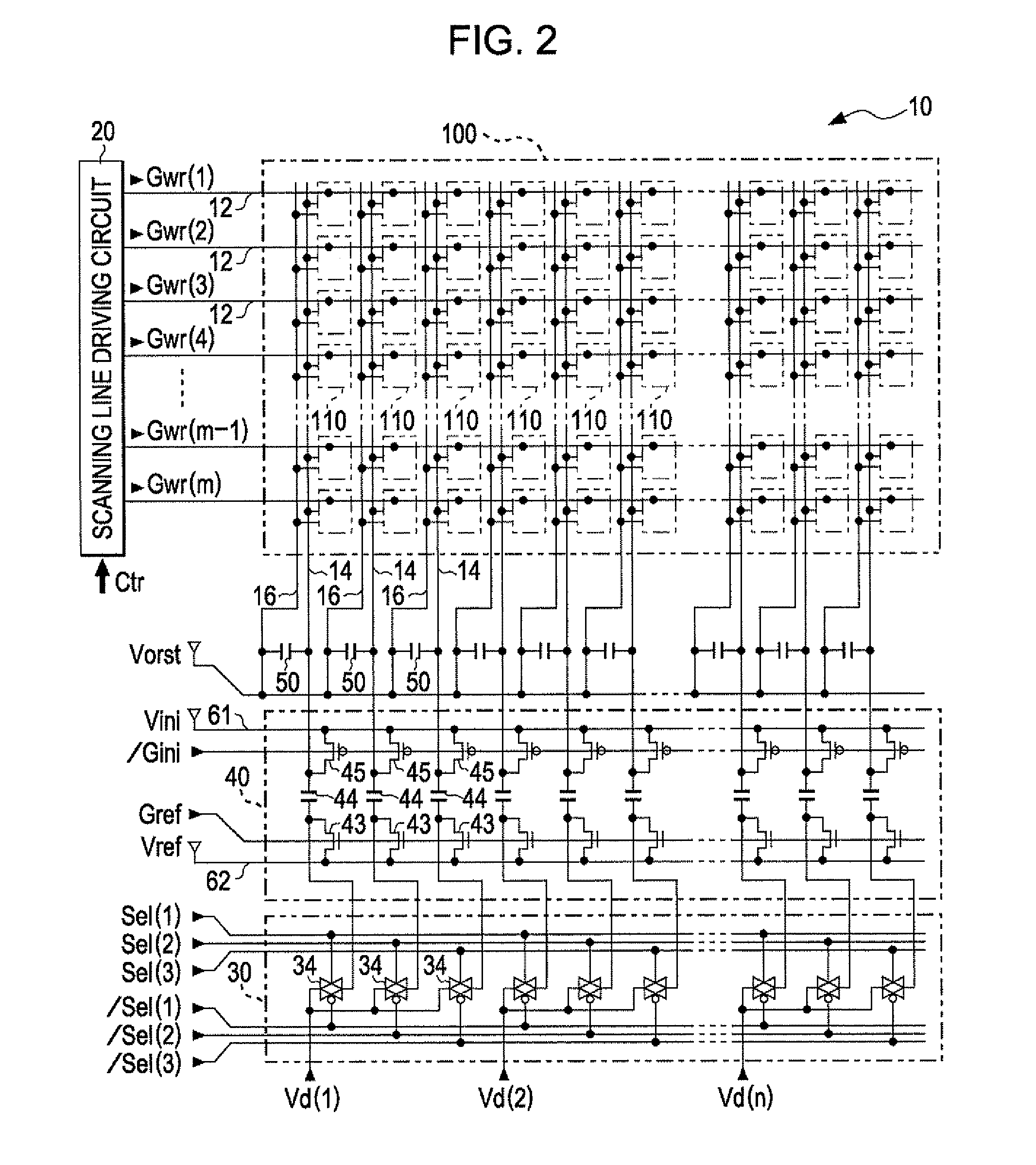
[0080]The operation of the electro-optical device 10 will be described with reference to FIG. 4. FIG. 4 is a timing chart for illustrating the operation of each part in the electro-optical device 10.

[0081]As shown in the drawings, the scanning signals Gwr(1) to Gwr(m) are sequentially switched to the L level and the scan lines 12 of rows 1 to m are scanned in order for each horizontal scanning period (H) in a period of one frame.

[0082]The operation in one horizontal scanning period (H) is common across the pixel circuits 110 of each row. Here, below, in the scanning period in which the i-th rows are horizontally scanned, description will be given of the operation with particular focus on the pixel circuit 110 of the i-th row, (3j−2)th column.

[0083]In the present embodiment, to make broad classifications, the scan period of the i-th row is divided into the initialization period shown by (b) in. FIG. 4, the compensation period shown by (c), and the writing...

second embodiment

Operation of Second Embodiment

[0134]The operation of the electro-optical device 10 according to the second embodiment will be described with reference to FIG. 12. FIG. 12 is a timing chart for illustrating the operation in the second embodiment.

[0135]As shown in the drawings, the point that the scanning signals Gwr(1) to Gwr(m) are sequentially switched to the L level and the scan lines 12 of rows 1 to m are scanned in order for each horizontal scanning period (H) in a period of one frame is the same as in the first embodiment. In addition, in the second embodiment, the point that the scanning period of the i-th row is made of an initialization period shown by (b), a compensation period shown by (c), and a writing period shown by (d) is also the same as the first embodiment. Here, the writing period of (d) in the second embodiment is a period from the time the control signal Gcpl changes from the L to the H level (when the control signal / Gcpl has become the L level) until the time ...

application and modification examples

[0171]The invention is not limited to the embodiments described above or the embodiments and the like of application examples, and, for example, various kinds of modifications as described below are possible. In addition, the forms of the modifications described below can be arbitrarily selected or a plurality thereof can be combined.

[0172]Control Circuit

[0173]In the embodiments, the control circuit 5 for supplying a data signal is separate from the electro-optical device 10; however, the control circuit 5 may be integrated into the silicon substrate along with the scanning line driving circuit 20, the demultiplexer 30, and the level shift circuit 40.

[0174]Substrate

[0175]In the embodiments, a configuration was adopted in which the electro-optical device 10 was integrated with a silicon substrate; however, a configuration of being integrated with another silicon substrate may be adopted. Further, the forming may be made in a glass substrate or the like by the application of a polysil...


PUM


Abstract

An electro-optical device includes a first storage capacitor that has a first electrode and a second electrode, and a second storage capacitor that has a third electrode and a fourth electrode, and a first pixel circuit. The first pixel circuit includes a first transistor having a first gate, a first drain, and a first source, an electro-optical element, a second transistor through which a first data line is electrically connected to the first gate during the second transistor is in an on-state, and a third transistor through which the first gate is electrically connected to the first drain or the first source. The second electrode and the third electrode are electrically connected to the first data line.

Description

BACKGROUND[0001]1. Technical Field[0002]The disclosed embodiments of the present invention relate to an electro-optical device, a driving method of an electro-optical device and an electronic apparatus effective when miniaturizing a pixel circuit, for example.[0003]2. Related Art[0004]In recent years, various kinds of electro-optical devices using light emitting elements such as organic light-emitting diode (Organic Light Emitting Diode, hereinafter referred to as “OLED”) elements have been proposed. In such electro-optical devices, generally, a pixel circuit corresponding to the intersections of scanning lines and data lines and including the above-described light emitting elements or transistors is configured so as to be provided to correspond to pixels in an image to be displayed. In such a configuration, when a data signal of a potential corresponding to the gradation level of pixels is applied to the gate of the transistor, the transistor supplies a current corresponding to the...

Claims


Application Information

Patent Timeline
Patent Type & Authority Applications(United States)
IPC IPC(8): G09G3/30
CPCG09G3/3233G09G2320/045G09G2300/0819G09G2300/0814G09G3/2096G09G3/3225G09G3/3291G09G3/3208G09G2300/0426G09G2310/0264G09G2310/08G09G2300/0439G09G3/3275
Inventor OTA, HITOSHIISHIGURO, HIDETO
Owner SEIKO EPSON CORP
Why Eureka
Try Eureka