Data recording system

a data recording and data technology, applied in the field of data recording systems, can solve the problems of inability to adopt the system, the limitation of the number of writes (the number of erase/write cycles) of the nonvolatile semiconductor memory, and the problems described in patent document 1 can not be overcome, so as to reduce the number of data writes to the first memory, prolong the life of the first memory, and reduce the cost of replacemen

Inactive Publication Date: 2011-02-01
FUJITSU LTD
View PDF8 Cites 8 Cited by
  • Summary
  • Abstract
  • Description
  • Claims
  • Application Information

AI Technical Summary

Benefits of technology

[0008]An object of the present invention is to extend the lifetime of a memory with a low-cost configuration in a data recording system.
[0010]In the above described configuration, an alarm is output if the number of data writes to the first memory exceeds a threshold value. Therefore, the need for replacing the first memory can be surely recognized, leading to the enhancement of the reliability of the data recording system. Additionally, the data of the number of writes is not recorded each time a data write to the first memory occurs, but recorded each time a predetermined condition is satisfied. Namely, the number of times that the data of the number of writes is written to the first or the second memory is reduced. Accordingly, the lifetime of the first memory can be extended in the configuration in which the data of the number of writes is written to the first memory. In the meantime, an alarm can be output without using the first memory in the configuration in which the data of the number of writes is written to the second memory.
[0013]In the above described configuration, the number of data writes to the first memory is reduced, thereby extending the lifetime of the first memory. Note that the lifetime of the second memory is not extended with this configuration. However, since the capacity of the second memory is small compared with the first memory, cost required for its replacement is low.
[0014]According to the present invention, the lifetime of a memory can be extended with a low-cost configuration in a data recording system.

Problems solved by technology

However, a limit number of writes (the number of erase / write cycles) of a nonvolatile semiconductor memory is normally small compared with a magnetic disk, etc.
However, the above described conventional techniques have problems to be overcome.
Namely, the configuration recited in Patent Document 1 cannot be adopted for a system that requires entire data to be stored, because part of collected data is discarded without being saved in a memory.
With the configuration recited in Patent Document 2, the capacity of a memory must be made large, leading to an increase in the cost.

Method used


Image

  • Data recording system
  • Data recording system
  • Data recording system

Examples


first embodiment

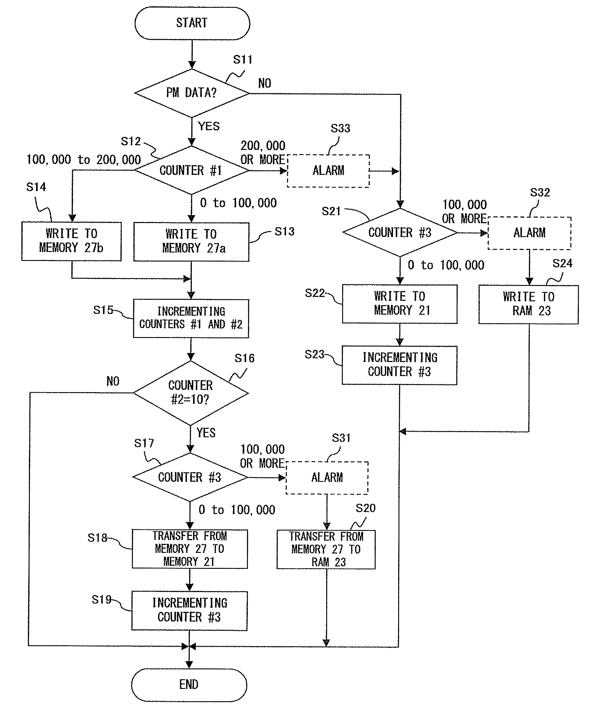
[0032]FIG. 4 is a block diagram showing a memory and its peripheral circuits. In this figure, the flash memory 21 is equivalent to the above described large-capacity memory, and is a nonvolatile memory. Although the flash memory 21 is a rewritable memory, its number of writes is limited. The limit number of writes (namely, a guaranteed maximum number of writes or the number of erase / write cycles) of the flash memory 21 is assumed to be 100,000 in this embodiment.

[0033]In the example shown in FIG. 4, a test tool program, an application program, FPGA data, provisioning data, PM data, and data of the number of writes (number-of-writes data) are stored in the flash memory 21. Although the FPGA data and the provisioning data are updated when necessary, their update frequencies are low. In the meantime, the PM data is written with high frequency since it is collected periodically as described above. The data of the number of writes represents the number of data writes to the flash memory ...

second embodiment

[0046]FIG. 6 shows a configuration of a data recording system according to a second embodiment. In the second embodiment, data of the number of writes is recorded not to a flash memory 21 but to another nonvolatile memory 26. The use frequency of the nonvolatile memory 26 is sufficiently low compared with the flash memory 21 in this embodiment. Accordingly, in the second embodiment, the frequency at which the data of the number of writes is recorded may be increased compared with the first embodiment shown in FIG. 4. Namely, the data of the number of writes may be recorded to the nonvolatile memory 26 once, for example, each time 100 data writes are made to the flash memory 21.

[0047]In the second embodiment, a parameter for managing the number of data writes of the flash memory 21 in the first embodiment is saved not in the flash memory 21 to be managed but in another nonvolatile memory, and a save operation is similar to the first embodiment.

third embodiment

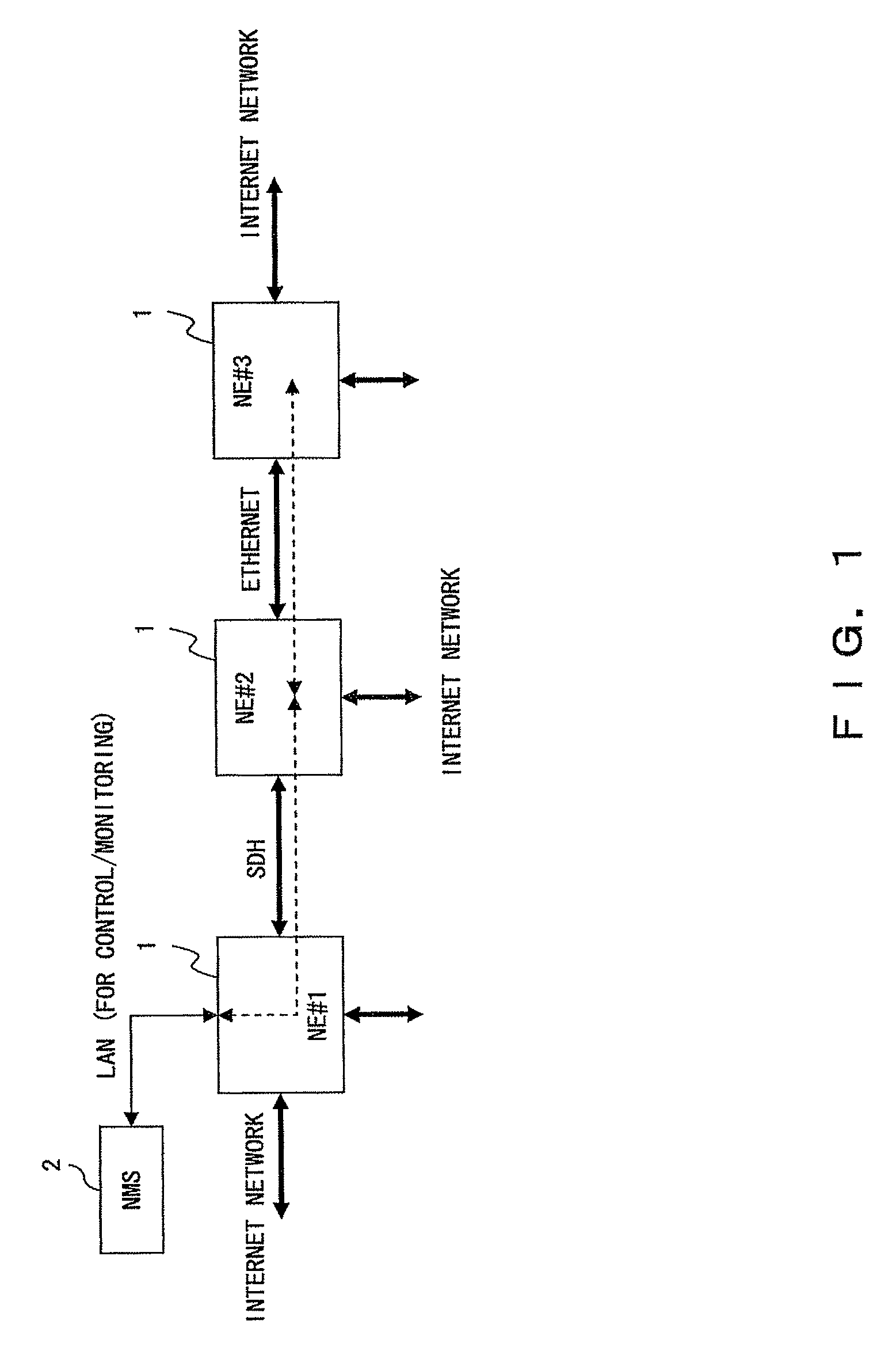
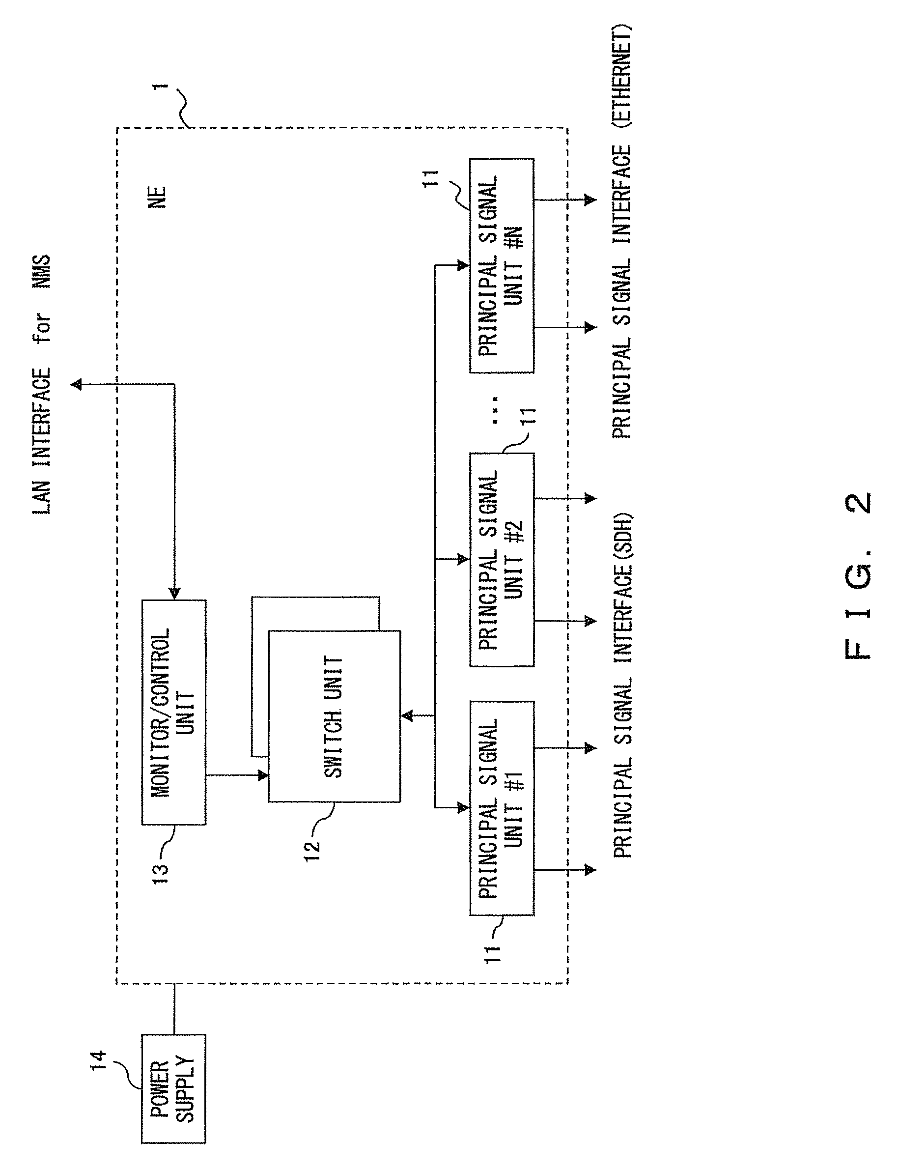
[0048]FIG. 7 shows a configuration of a data recording system according to a third embodiment. In the third embodiment, data of the number of writes is periodically transmitted from a CPU 24 to a network management system 2 without being recorded in the flash memory 21. Here, the data of the number of writes may be transmitted by request made from the network management system 2, or the CPU 24 may autonomously transmit the data of the number of writes. Then, the network management system 2 outputs an alarm if the data of the number of writes exceeds a threshold value.


PUM


Abstract

A data recording system comprises a first memory, a counting unit for counting the number of data writes to the first memory, and an alarm unit for outputting an alarm if the number of data writes to the first memory reaches a first threshold value. The counting unit writes data of the number of writes, which represents the number of data writes to the first memory, to the first memory or a second memory. The alarm unit outputs an alarm based on the data of the number of writes, which is written to the first or the second memory.

Description

BACKGROUND OF THE INVENTION[0001]1. Field of the Invention[0002]The present invention relates to a data recording system that uses a memory having a limitation on the number of writes.[0003]2. Description of the Related Art[0004]Memories for saving data are in widespread use in a variety of fields. Especially, the capacities of nonvolatile semiconductor memories (such as a flash memory, an EEPROM, a PROM, etc.) have been increased, and their intended uses have expanded in recent years. Semiconductor memories are normally superior in resistance to vibration, and low power consumption compared with other nonvolatile memories such as a magnetic disk, etc.[0005]However, a limit number of writes (the number of erase / write cycles) of a nonvolatile semiconductor memory is normally small compared with a magnetic disk, etc. For this reason, the number of writes of a nonvolatile semiconductor memory can reach the limit number if the data of the memory is frequently updated for a long period. ...

Claims


Application Information

Patent Timeline
Patent Type & Authority Patents(United States)
IPC IPC(8): G06F12/00
CPCG06F11/1076G11C16/349
Inventor RIKITAKE, NOBUHIRO
Owner FUJITSU LTD
Why Eureka
Try Eureka