Nitride semiconductor light emitting device

a light-emitting device and semiconductor technology, applied in the direction of semiconductor devices, basic electric elements, electrical equipment, etc., can solve the problems of increasing current flow, increasing the value of vf, and reducing the efficiency of light-emitting due to light absorption, so as to achieve uniform light-emitting, reduce the value of vf, and achieve sufficient luminous intensity of emission

Active Publication Date: 2011-02-08
NICHIA CORP
View PDF22 Cites 6 Cited by
  • Summary
  • Abstract
  • Description
  • Claims
  • Application Information

AI Technical Summary

Benefits of technology

[0011]With the background described above, the present invention has an object of providing a nitride semiconductor light emitting device having a translucent electrode formed from an electrically conductive oxide, which is capable of improving the uniformity of light emission and decreasing the value of Vf, without forming long extensions from the n-side pad electrode and the p-side pad electrode.
[0014]Through a research conducted by the inventors of the present application, it was found that the uniformity of light emission can be improved and the value of Vf can be decreased while maintaining sufficient luminous intensity of emission and sufficient endurance for electrostatic breakdown of the device, by forming the p-side pad electrode at a position a little inward of the translucent electrode, namely at a position that satisfies the relationships described above, particularly when the translucent electrode is formed from an electrically conductive oxide. This is because, since the translucent electrode formed from an electrically conductive oxide tends to have higher sheet resistance than that of the n-type nitride semiconductor layer, current which would otherwise be concentrated around the p-side pad electrode can be spread uniformly throughout the device plane by forming the p-side pad electrode at a position a little inward of the translucent electrode. Particularly it is preferable that X and Y satisfy the following relationship, which enables it to provide a device that emits light with higher uniformity and has lower value of Vf.0.5L≦X≦0.6L and 0.3L≦Y≦0.5L
[0015]The nitride semiconductor light emitting device of the present invention preferably has a plurality of protrusions formed from at least the p-type nitride semiconductor layer along the periphery of the device. This makes it possible to further improve the uniformity of light emission due to the arrangement of the p-side pad electrode, thereby to have the entire surface of the device contribute effectively to light emission.
[0016]It is also preferable that top surface of the substrate has irregularity so as to suppress multiple reflections of light within the device, thereby improving the efficiency of extracting light.
[0017]According to the present invention, as described above, it is made possible to provide the nitride semiconductor light emitting device which has the translucent electrode formed from the electrically conductive oxide and is capable of improving the uniformity of light emission and decreasing the value of Vf, without forming long extensions from the n-side pad electrode and from the p-side pad electrode.

Problems solved by technology

As a result, such a problem can easily occur that current flows more around the p-side pad electrode and less around the n-side pad electrode.
Uneven current distribution within the element plane may lead to a problem related to the electrical characteristic such as higher value of Vf (forward voltage).
Also, the problem described above becomes more significant as the shape of the device becomes more proximate to rectangle.
Thus simply forming the linear extensions from the n-side pad electrode and from the p-side pad electrode leads to smaller area of light emission as the extensions become longer, thus resulting in a decrease in the efficiency of light emission due to the absorption of light.

Method used


Image

  • Nitride semiconductor light emitting device
  • Nitride semiconductor light emitting device
  • Nitride semiconductor light emitting device

Examples


Embodiment Construction

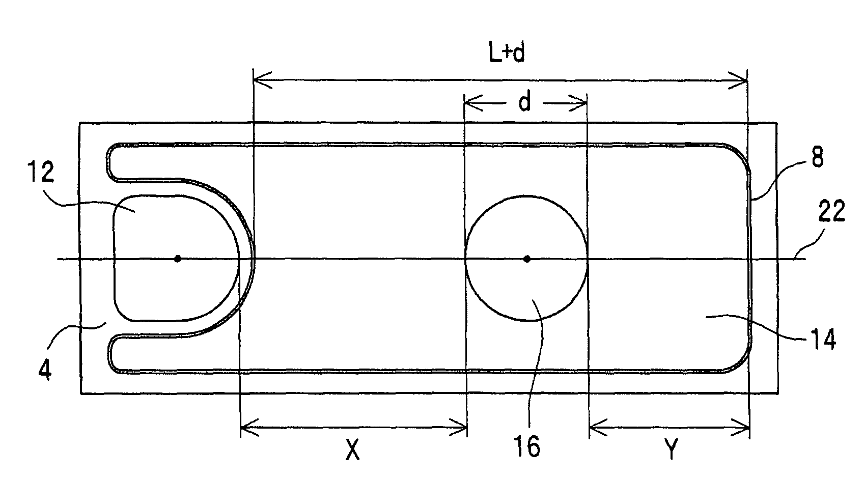
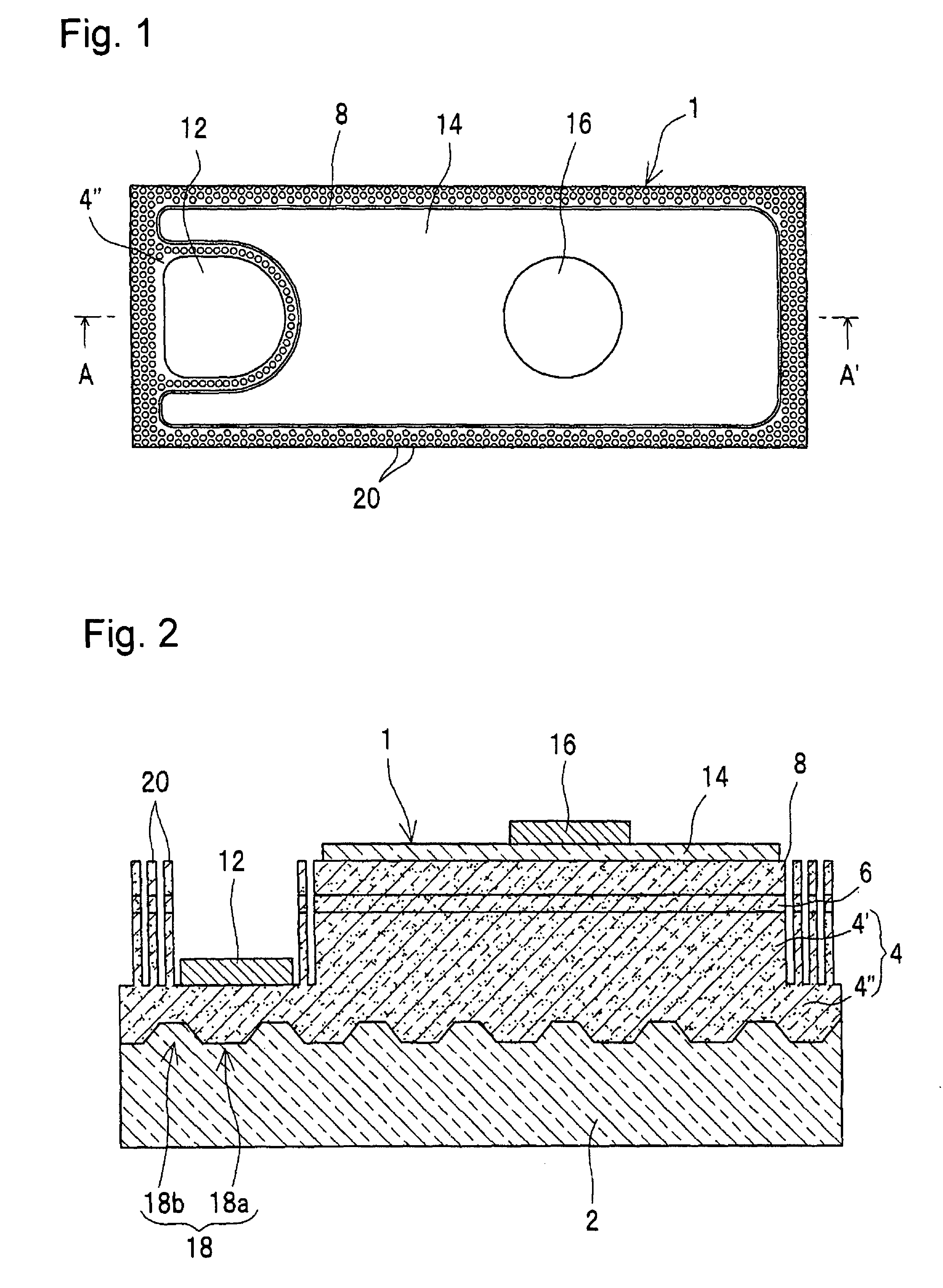
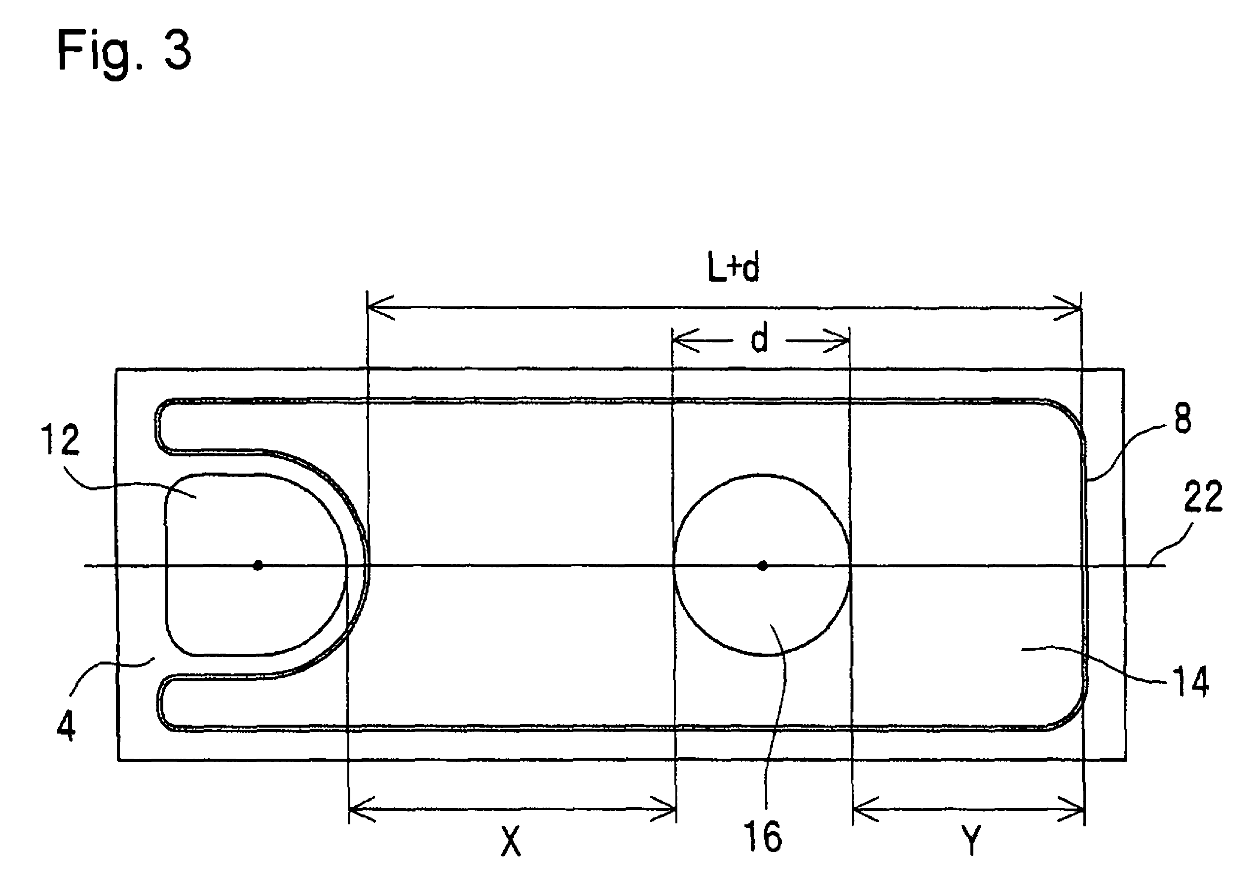
[0057]FIG. 1 is a top view showing an example of the nitride semiconductor light emitting device of the present invention. FIG. 2 is a sectional view taken along lines A-A′ of FIG. 1. As shown in FIG. 1, the nitride semiconductor light emitting device of this embodiment has rectangular shape of a large aspect ratio in plan view, with the n-side pad electrode 12 and the p-side pad electrode 16 disposed along the linger side of the rectangle. The nitride semiconductor light emitting device 1 has double-heterojunction structure constituted by forming an n-type nitride semiconductor layer 4, an active layer 6 and a p-type nitride semiconductor layer 8 one on another on a substrate 2 made of sapphire, SiC, GaN or the like. In this embodiment, since the active layer 6 is formed from n-type nitride semiconductor layer, both the n-type nitride semiconductor layer and the active layer 6 correspond to the n-type nitride semiconductor layer of the present invention.

[0058]The p-type nitride sem...


PUM


Abstract

A nitride semiconductor light emitting device is provided with a substrate, an n-type nitride semiconductor layer, a p-type nitride semiconductor layer, an n-side pad electrode, a translucent electrode and a p-side pad electrode, wherein the translucent electrode is formed from an electrically conductive oxide, the n-side pad electrode adjoins the periphery of the translucent electrode and the p-side pad electrode is disposed so as to satisfy the following relationships:0.3L≦X≦0.5L and 0.2L≦Y≦0.5Lwhere X is the distance between ends of the p-side pad electrode and the n-side pad electrode, Y is the distance between the end of the p-side pad electrode and the periphery of the translucent electrode, L is the length of the translucent electrode on the line connecting the centroids of the p-side pad electrode and the n-side pad electrode minus the outer diameter d of the p-side pad electrode.

Description

BACKGROUND OF THE INVENTION[0001]1. Field of the Invention[0002]The present invention relates a nitride semiconductor light emitting device comprising a nitride semiconductor represented by general formula of InxAlyGa1-x-yN (0≦x<1, 0≦y<1), and particularly to a nitride semiconductor light emitting device having an n-side pad electrode and a p-side pad electrode formed on the same side of a substrate.[0003]2. Description of the Related Art[0004]A nitride semiconductor light emitting device commonly used is constituted by forming at least an n-type nitride semiconductor layer and a p-type nitride semiconductor layer one on another on a substrate made of sapphire, SiC, GaN or the like. The p-type nitride semiconductor layer has a p-side pad electrode formed thereon for connecting to a positive terminal of an external power source, and the n-type nitride semiconductor layer has an n-side pad electrode formed thereon for connecting to a negative terminal of the external power sourc...

Claims


Application Information

Patent Timeline
Patent Type & Authority Patents(United States)
IPC IPC(8): H01L29/205H01L31/12H01L29/165H01L27/15H01L33/00H01L33/10H01L33/22H01L33/32H01L33/38H01L33/42H01L33/50H01L33/56
CPCH01L33/38H01L33/20H01L2224/48091H01L2924/00014
Inventor SAKAMOTO, TAKAHIKOHAMAGUCHI, YASUTAKA
Owner NICHIA CORP
Why Eureka
Try Eureka