

Resistance change memory device
a memory device and resistance change technology, applied in semiconductor devices, digital storage, instruments, etc., can solve the problems of affecting the operation of the device, and it is difficult to make the cell be in a set operation mode and the other cell in a reset operation mode simultaneously
- Summary
- Abstract
- Description
- Claims
- Application Information
AI Technical Summary
Benefits of technology
Problems solved by technology
Method used
Image

Examples
embodiment 1
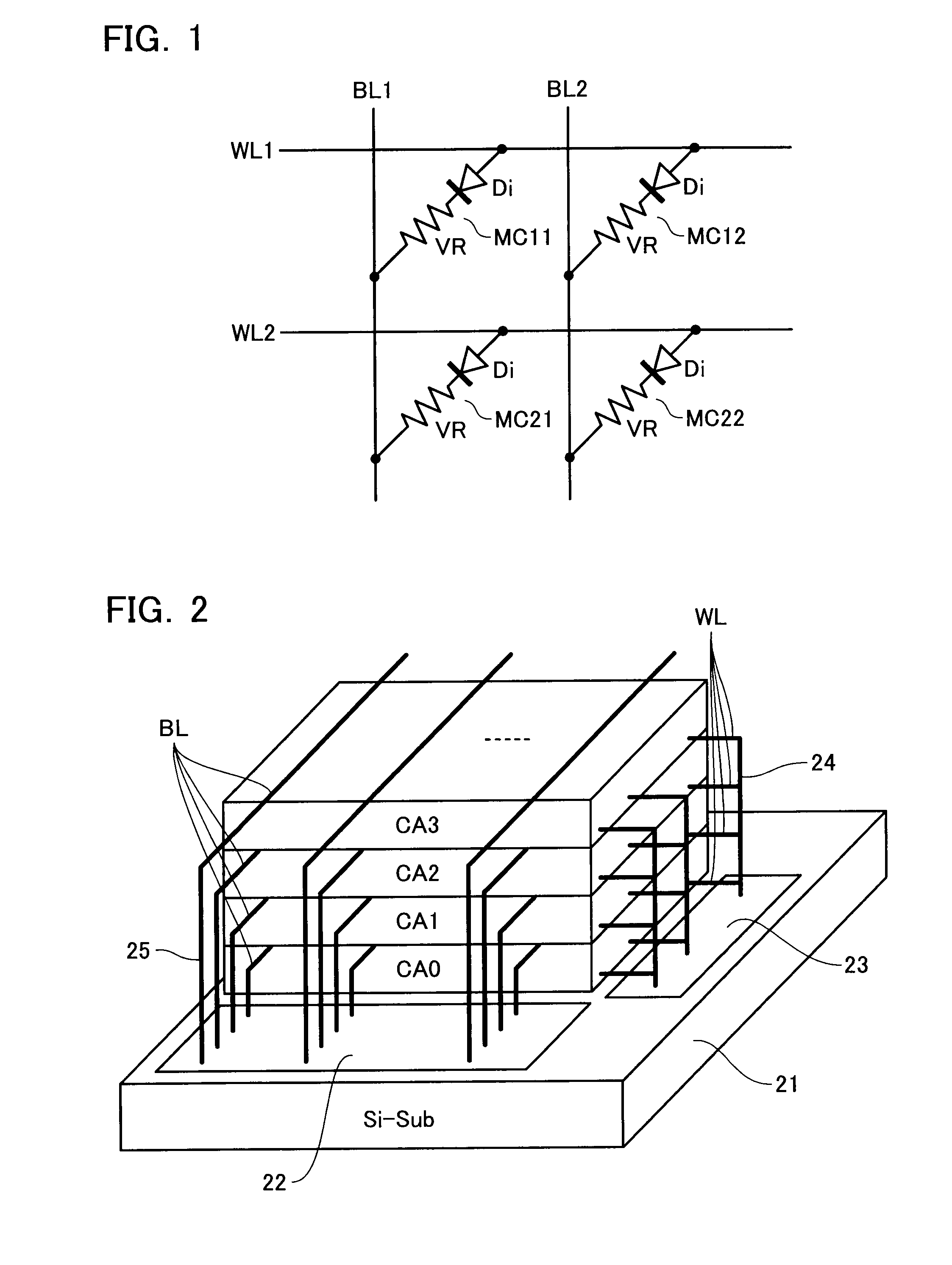
[0034]FIG. 1 shows an equivalent circuit of a cell array of a resistance change memory in accordance with an embodiment. Bit lines BL (BL1, BL2, . . . ) and word lines WL (WL1, WL2, . . . ) are disposed to cross each other, and memory cells MC (MC11, MC12, . . . , MC21, MC22, . . . ) are disposed at the respective cross-points of the bit lines BL and word lines WL.
[0035]Memory cell MC is formed of a variable resistance element VR and a diode Di connected in series. Variable resistance element VR stores a resistance value as data in a non-volatile manner, which is reversibly settable with an electrical or thermal process. Although the detailed layout is not shown, for example, diode Di and variable resistance element VR are stacked on word lines WL, and bit lines BL are formed thereon in perpendicular to the word lines WL.
[0036]To achieve a resistance change memory with a large capacity, as shown in FIG. 2, multiple cell arrays are stacked to constitute a three-dimensional (3D-) cell...
embodiment 2
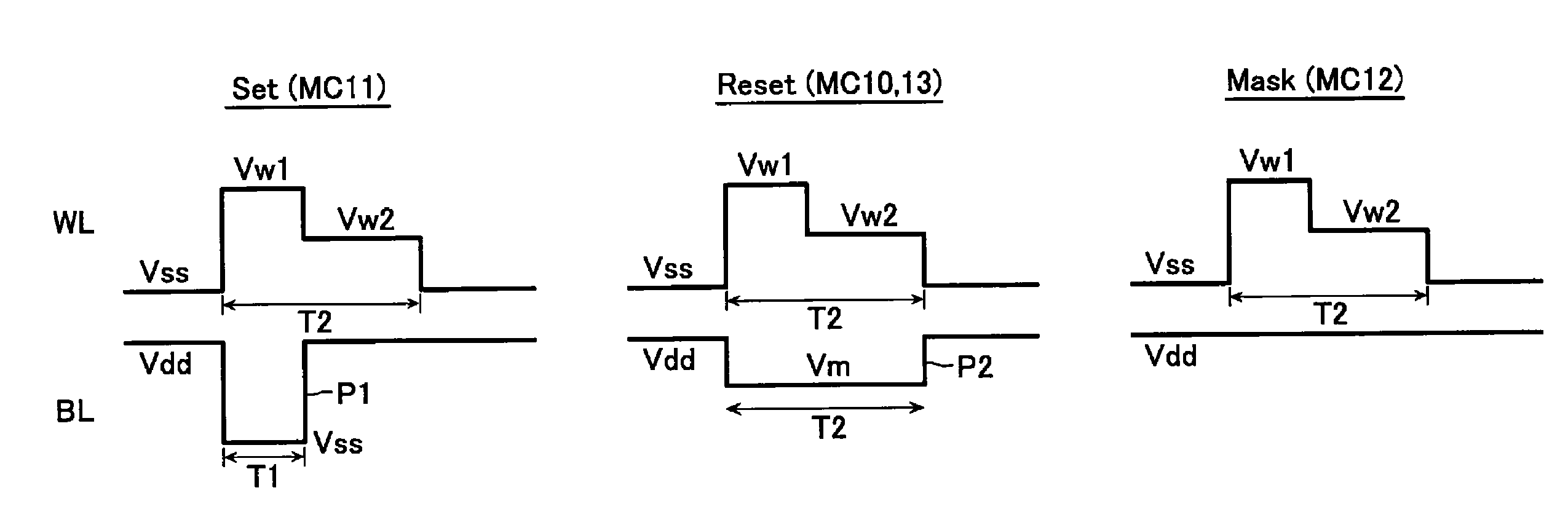
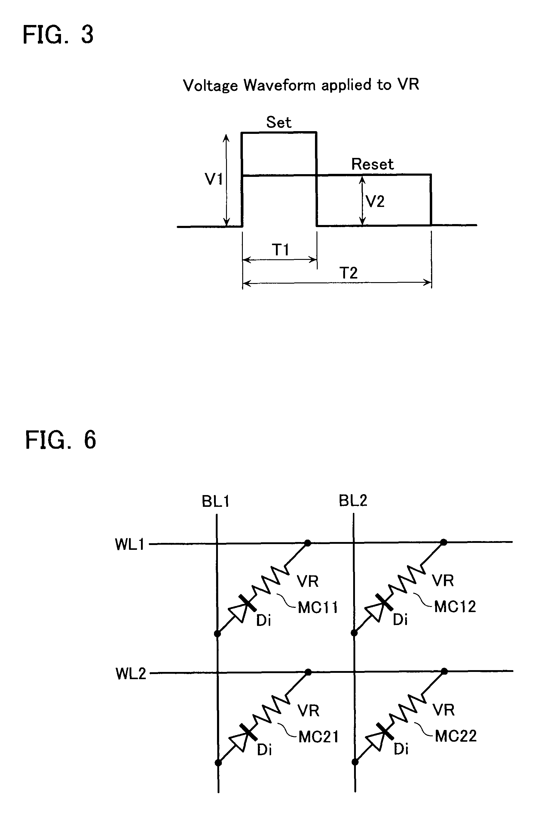
[0053]FIG. 6 shows another cell array arrangement, in which the diode polarity is reversed to that shown in FIG. 1. That is, in this case, when a bit line is relatively higher than a word line, a memory cell is selected at the cross-point of the word line and the bit line. In this case, voltage waveforms in the set, reset and mask modes are shown in FIG. 7 in comparison with those shown in FIG. 5.
[0054]That is, a selected word line is applied with a composite pulse composed of a negative pulse with pulse width T1, which swings from the basic level Vdd to Vss, and another negative pulse with pulse width T2, which swings from the basic level Vdd to a medium level Vm (Vdd>Vm>Vss). Bit line BL is applied with; set-use pulse P1′, which is positive voltage Vw1 with pulse width T1 on the basic level Vss, in the set mode; reset-use pulse P2′, which is positive voltage Vw2 with pulse width T2 on the basic level Vss, in the reset mode; and Vss in the mask mode.
[0055]As a result, multiple cell...
embodiment 3
[0056]FIG. 8 shows another embodiment, in which it is made possible to write a certain data pattern in multiple memory cells in a two-dimensional cell array at once. The cell array configuration (i.e., diode polarity) is the same as in the embodiment 1. Word line driver circuit 71 has mode selecting circuits 71a (71a0, 71a1, . . . ) disposed for the respective word lines and multiplexers 71b (71b0, 71b1, . . . ) controlled by the mode selecting circuits 71a, as similar to the bit line driver circuit.
[0057]In detail, the mode selecting circuit 71a is for selecting data writing mode (including set and reset modes) and mask mode, and formed of a data register storing one bit data. Write-use voltage signal line 76 and mask-use voltage signal line 77 are prepared to be shared by the plural word lines, and these signal lines are selectively coupled to word lines WL via transistors Q4 or Q5 driven by the multiplexers 71b, so that write-use voltage (i.e., selecting drive voltage) and mask-u...
PUM
 Abstract
Description
Claims
Application Information