
Enhancement of input/output for non source-synchronous interfaces

a non-source-synchronous interface and input/output technology, applied in the field of electrical interfaces, can solve problems such as interface changes, unpractical use of approaches in many devices,

Inactive Publication Date: 2011-02-15
SANDISK TECH LLC
View PDF7 Cites 20 Cited by
  • Summary
  • Abstract
  • Description
  • Claims
  • Application Information

AI Technical Summary

Benefits of technology

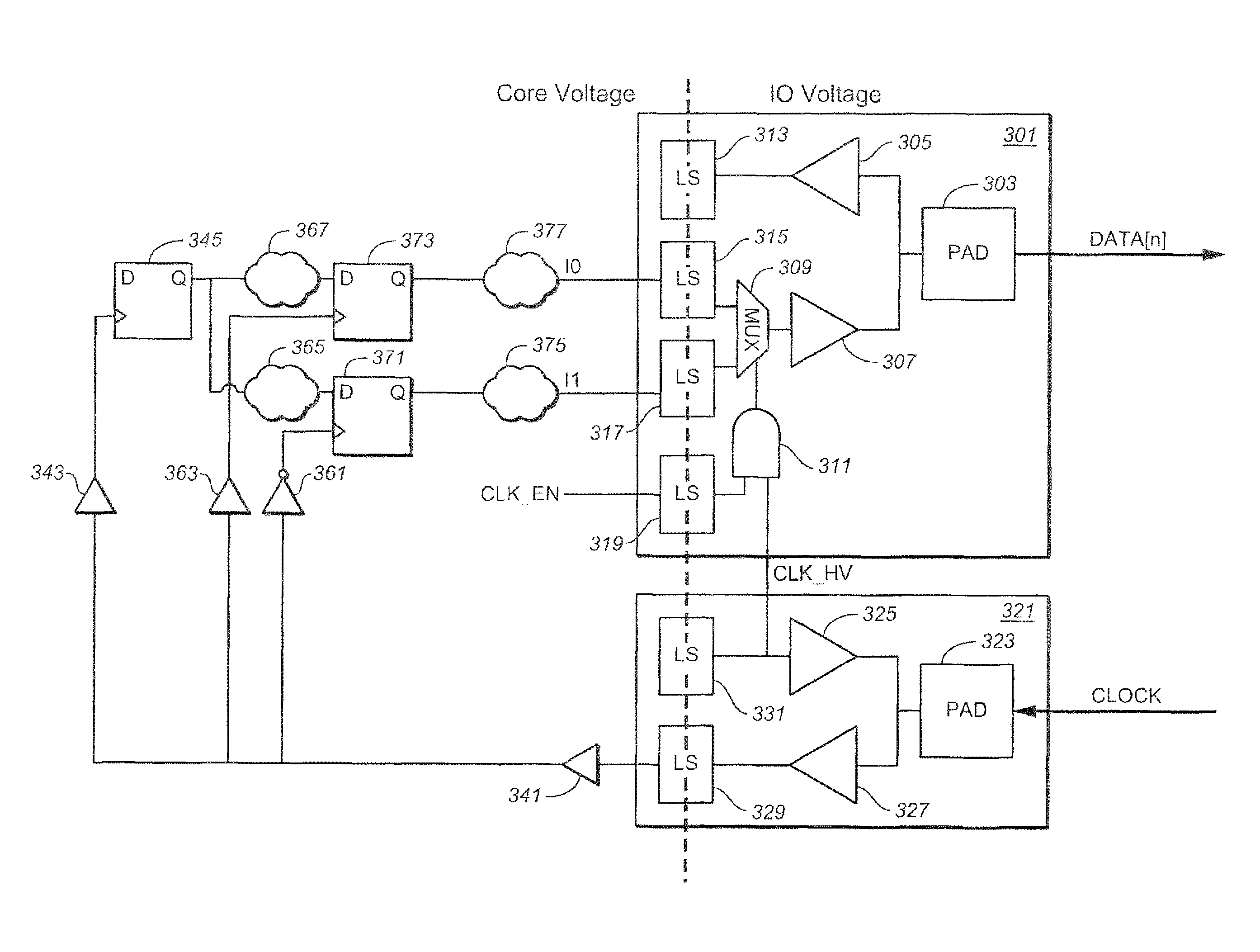
The patent describes an interface circuit and method for connecting two devices with different voltage ranges. The interface circuit has multiple input / output cells with level shifting circuits to convert signals between the two ranges. The input / output cells include a first input / output cell to receive a clock signal and data signals from the second device, level shift the signals to the first range, and provide them to the first device's core processing circuitry. The interface circuit also includes a second input / output cell to receive the data signals and convert them to the second range. The interface circuit generates a double data rate signal by combining the data signals and the clock signal. The technical effect of this invention is to enable seamless connectivity and efficient data transfer between devices with different voltage ranges.

Problems solved by technology

However, this approach may not be practical to use in many devices as it may incur substantial changes to the interface (e.g. addition of signal pins).

Method used


Image

  • Enhancement of input/output for non source-synchronous interfaces
  • Enhancement of input/output for non source-synchronous interfaces
  • Enhancement of input/output for non source-synchronous interfaces

Examples


Embodiment Construction

[0012]The following presents an interface, and corresponding techniques, for use of device whose core circuitry operates in one voltage domain, but exchanges signal with another device (or “host”) according a different voltage domain; and the use of such an interface for supplying data using a double data rate (DDR) transfer. A concrete example of this situation is a memory card, where the internal circuitry uses one voltage range for its core operating voltages, but exchanges signals with a host using different, input / output voltage range. According to a general set of aspects presented below, the interface receives data signals from the device at the device's core operating voltage domain, individually level shifts these to the input / output voltage domain, and then combines them into a DDR signal for transfer to the host device, where a (non-level shifted) clock signal from the host device is used as the select signal to form the DDR data signal.

[0013]As discussed in the Backgroun...


PUM


Abstract

An interface for use of device whose core circuitry operates in one voltage domain, but exchanges signal with another device (or “host”) according a different voltage domain, and the use of such an interface for supplying data using a double data rate (DDR) transfer, is presented. One concrete example of this situation is a memory card, where the internal circuitry uses one voltage range for its core operating voltages, but exchanges signals with a host using different, input / output voltage range. According to a general set of aspects, the interface receives data signals from the device at the device's core operating voltage domain, individually level shifts these to the input / output voltage domain, and then combines them into a DDR signal for transfer to the host device, where a (non-level shifted) clock signal from the host device is used as the select signal to form the DDR data signal.

Description

FIELD OF THE INVENTION[0001]This invention pertains generally to the field of electrical interfaces and, more particularly, to the output of data for non source-synchronous interfaces.BACKGROUND[0002]A simple interface for the purpose of data transfer between integrated circuit devices will often include a clock signal provided by the host device which is used by the slave device to output data to the host. A specific example is a read cycle of a memory card or other memory device by a host. The timing of the data output from the slave is then dependent on the arrival of the clock signal. There is an ongoing process to increase of performance of such devices. When higher transfer speeds are desired, one approach is to migrate an interface protocol to a source-synchronous scheme where the both the clock and data signals are provided from the same device, such as in a DDR (Double Data Rate) arrangement used in DRAM devices. However, this approach may not be practical to use in many de...

Claims


Application Information

Patent Timeline
Patent Type & Authority Patents(United States)
IPC IPC(8): H03K19/0175H03K19/00
CPCG11C7/10G11C7/1066G11C16/10
Inventor DAVIDSONHERON, RALPHIGUELMAMENE, LAKHDARTAL, RONYDRUCK, ASHER
Owner SANDISK TECH LLC
Learn More