Charged balanced devices with shielded gate trench

a balanced device and gate trench technology, applied in the direction of semiconductor devices, basic electric elements, electrical apparatus, etc., can solve the problems of less desirable floating islands and slow electrical transitions, and achieve the effects of reducing channel performance sensitivity, slow electrical transitions, and good control of transistor cell performan

a balanced device and gate trench technology, applied in the direction of semiconductor devices, basic electric elements, electrical apparatus, etc., can solve the problems of less desirable floating islands and slow electrical transitions, and achieve the effects of reducing channel performance sensitivity, slow electrical transitions, and good control of transistor cell performan

US7893488B2Active Publication Date: 2011-02-22ALPHA & OMEGA SEMICON INC

Image

  • Charged balanced devices with shielded gate trench
  • Charged balanced devices with shielded gate trench
  • Charged balanced devices with shielded gate trench

Examples


Embodiment Construction

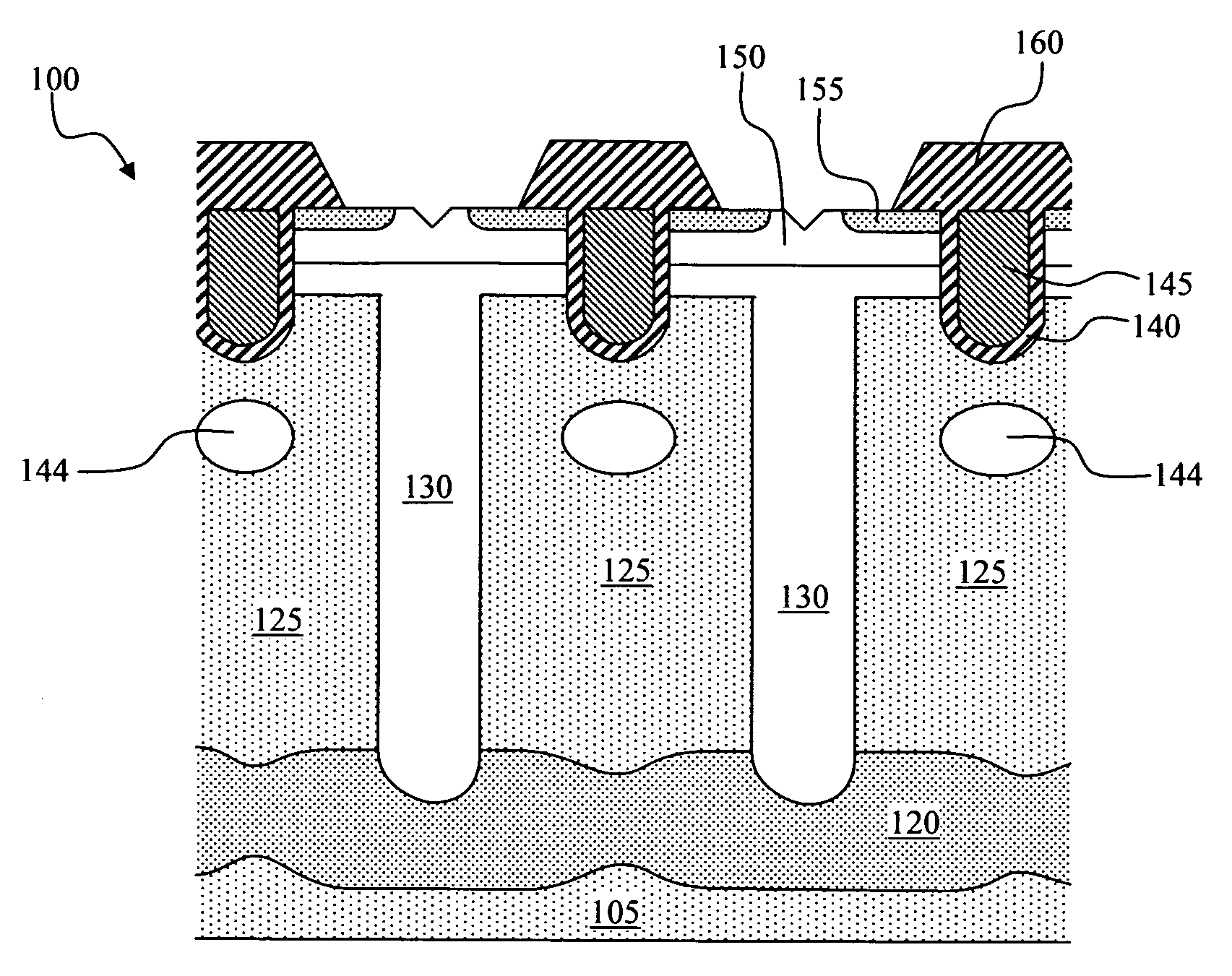
[0030]Referring to FIG. 2 for a cross sectional view of a MOSFET device 100 that illustrates the new concepts including the new structural and manufacturing features of this invention. The details of the MOSFET device 100 will be further described and explained in FIG. 3 below. The MOSFET device 100 is supported on a substrate 105 that includes an N+ doped bottom region 120 functioning as drain contact region doped through deep trenches 130 (after back-grinding, as shown in FIG. 3 below) that is filled with an epitaxial layer therein. The substrate 105 may include a top portion 125 in which the deep trenches 130 are formed. For the example of an n-channel MOSFET, the substrate 105 is n-type, and the epitaxial layer in the deep trenches 130 is p-type. The MOSFET transistor cells are supported on the single thin epitaxial layer filling in epitaxial column trenches 130 and covering over the top surface surrounding the P-epitaxial columns that has the P-epitaxial filling in the column t...


PUM


Abstract

This invention discloses a semiconductor power device disposed on a semiconductor substrate includes a plurality of deep trenches with an epitaxial layer filling said deep trenches and a simultaneously grown top epitaxial layer covering areas above a top surface of said deep trenches over the semiconductor substrate. A plurality of trench MOSFET cells disposed in said top epitaxial layer with the top epitaxial layer functioning as the body region and the semiconductor substrate acting as the drain region whereby a super-junction effect is achieved through charge balance between the epitaxial layer in the deep trenches and regions in the semiconductor substrate laterally adjacent to the deep trenches. Each of the trench MOSFET cells further includes a trench gate and a gate-shielding dopant region disposed below and substantially aligned with each of the trench gates for each of the trench MOSFET cells for shielding the trench gate during a voltage breakdown.

Description

[0001]This Patent Application is a Continuation in Part (CIP) Application of Ser. No. 12 / 229,250 filed by a common Inventor of this Application on Aug. 20, 2008 now U.S. Pat. No. 7,790,549. The disclosure made in that Application is hereby incorporated by reference.BACKGROUND OF THE INVENTION[0002]1. Field of the Invention[0003]The invention relates generally to vertical semiconductor power devices. More particularly, this invention relates to configurations and methods implemented with a single thin epitaxial layer with improved manufacturability for manufacturing flexibly scalable charge balanced vertical semiconductor power devices with a super-junction structure and shielded gate trench with simple manufacturing processes flexibly adjustable for applications to different targeted breakdown voltages.[0004]2. Description of the Prior Art[0005]Conventional manufacturing technologies and device configuration to further increase the breakdown voltage with reduced series resistance ar...

Claims


Application Information

Patent Timeline
22 Feb 2011
Publication
US7893488B2
IPC
H01L29/66
CPC
H01L29/0623; H01L29/0634; H01L29/66734; H01L29/7813; H01L21/26586; H01L29/0696; H01L29/0873; H01L29/0878
Inventors
HEBERT, FRANCOIS