Method for manufacturing semiconductor device

a manufacturing method and semiconductor technology, applied in the direction of semiconductor devices, basic electric elements, electrical appliances, etc., can solve the problems of increasing leak current, increasing power consumption, and poor insulation performance of more than 2 nm, and simplifying the removal step of the film, reducing the adverse effect of the devi

Active Publication Date: 2011-03-01
TOKYO ELECTRON LTD
View PDF16 Cites 0 Cited by
  • Summary
  • Abstract
  • Description
  • Claims
  • Application Information

AI Technical Summary

Benefits of technology

[0015]The present invention has been made taking account of the above-described problems to effectively solve the same. The object of the present invention is to provide a method of manufacturing a semiconductor device, which is capable of efficiently, reliably removing an SiC-based film of a multilayer structure having both an anti-reflective function and a hardmask function, while simplifying a removing step of the film in a gate electrode forming process, thereby reducing an adverse effect on the device as much as possible.
[0018]According to these inventions, the SiC-based film can be efficiently, reliably removed by a combination of the plasma-processing step and the cleaning step. Further, removal of the SiC-based film and removal of the High-k film can be collectively conducted in a single step. Since the number of steps can be reduced, throughput in a process for forming a gate electrode of a transistor and so on can be improved, while manufacturing costs can be reduced.
[0019]Since two types of films of different functions can be removed in a single removing step, deterioration in a device caused by a plasma damage can be prevented as much as possible. In addition, side edges of a gate insulation film and film-reduction of a buried insulation film (BOX) can be restrained as much as possible. As a result, deterioration in device properties and lowering of throughput can be significantly prevented.

Problems solved by technology

However, a silicon oxide film having a thickness of not more than 2 nm has a poor insulation performance, so that a leak current is increased.
With increase in the gate leak current, a power consumption is significantly increased.
In addition, because of a thinner gate insulation film, there is a possibility that impurities such as boron are dispersed from a gate electrode into the gate insulation film.
This phenomenon impairs the performance and the reliability of the transistor.
However, the use of a High-k film in a manufacturing process of a semiconductor device has not been long, there is a lot of room for improvement.
A chemical agent such as hydrofluoric acid (HF), which has been conventionally used for removing a gate insulation film (SiO2), cannot directly remove the annealed High-k film.
However, the reduced thickness of the photoresist film may simultaneously make it difficult to accurately etch the film.
However, in this conventional method of laying a hardmask under the ARC film, an anti-reflective function is not always sufficient, and thus a sufficient resolution and a sufficient lithography process tolerance may not be provided.
Such an increased number of steps invites problems such as deterioration in a device caused by a plasma damage, side-etching of a gate insulation film in a wet cleaning step, and film-reduction of a buried insulation film.
9H) may give an adverse effect on a semiconductor device.

Method used


Image

  • Method for manufacturing semiconductor device
  • Method for manufacturing semiconductor device
  • Method for manufacturing semiconductor device

Examples


Embodiment Construction

[0034]Embodiments of a method of manufacturing a semiconductor device according to the present invention will be described below with reference to the accompanying drawings.

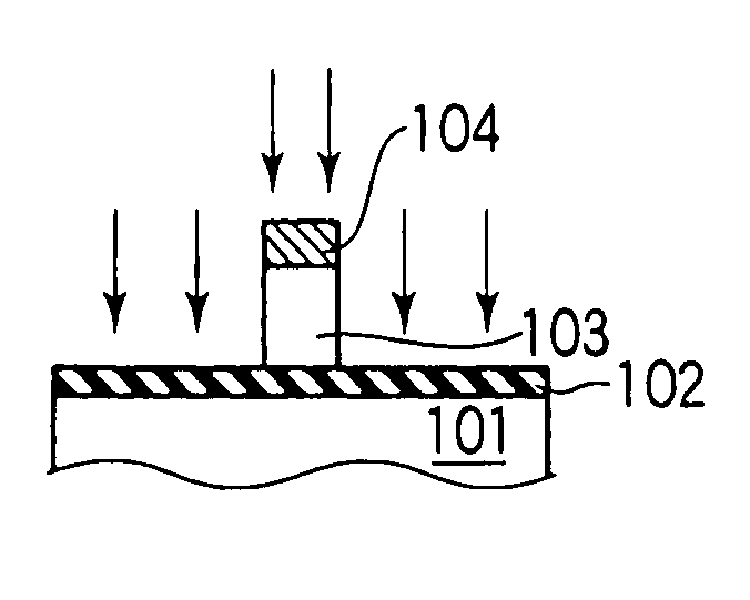
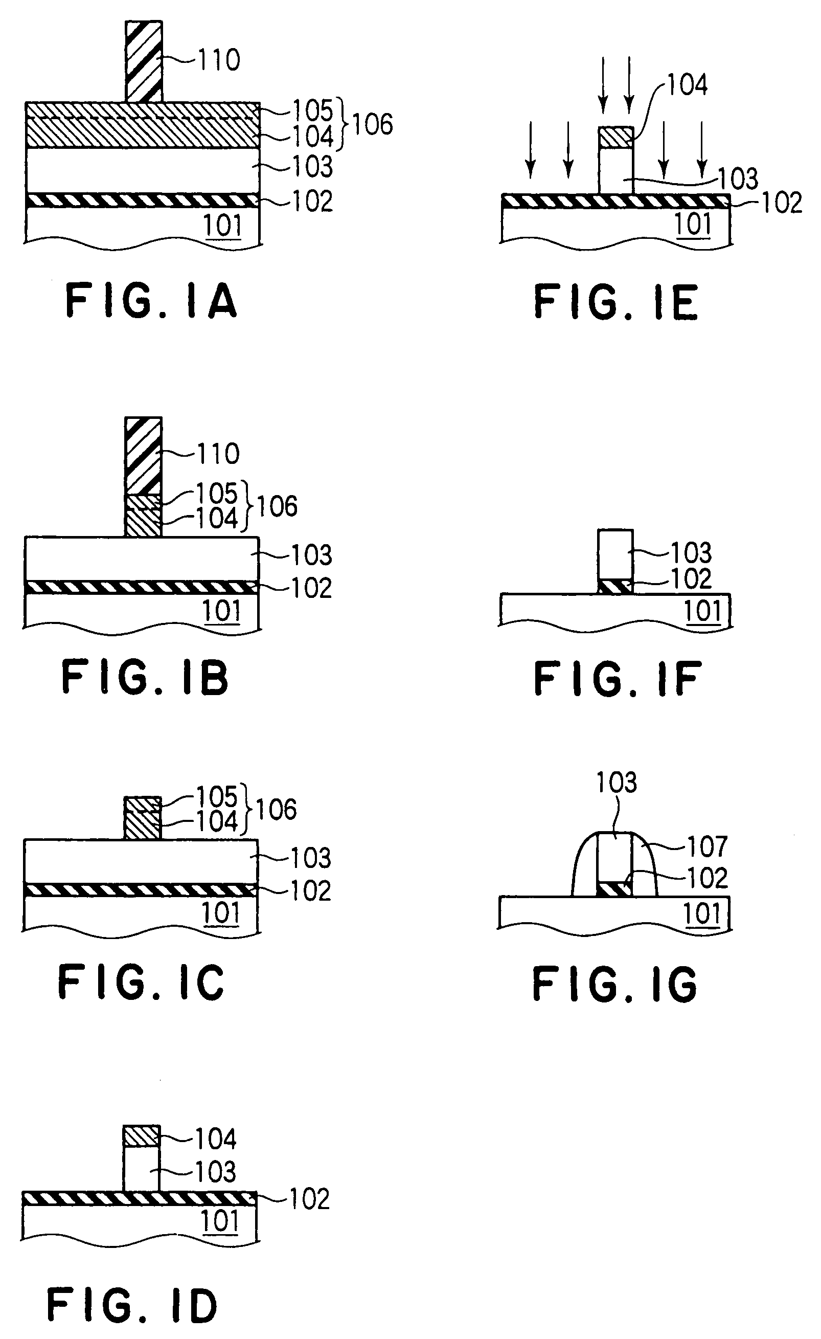
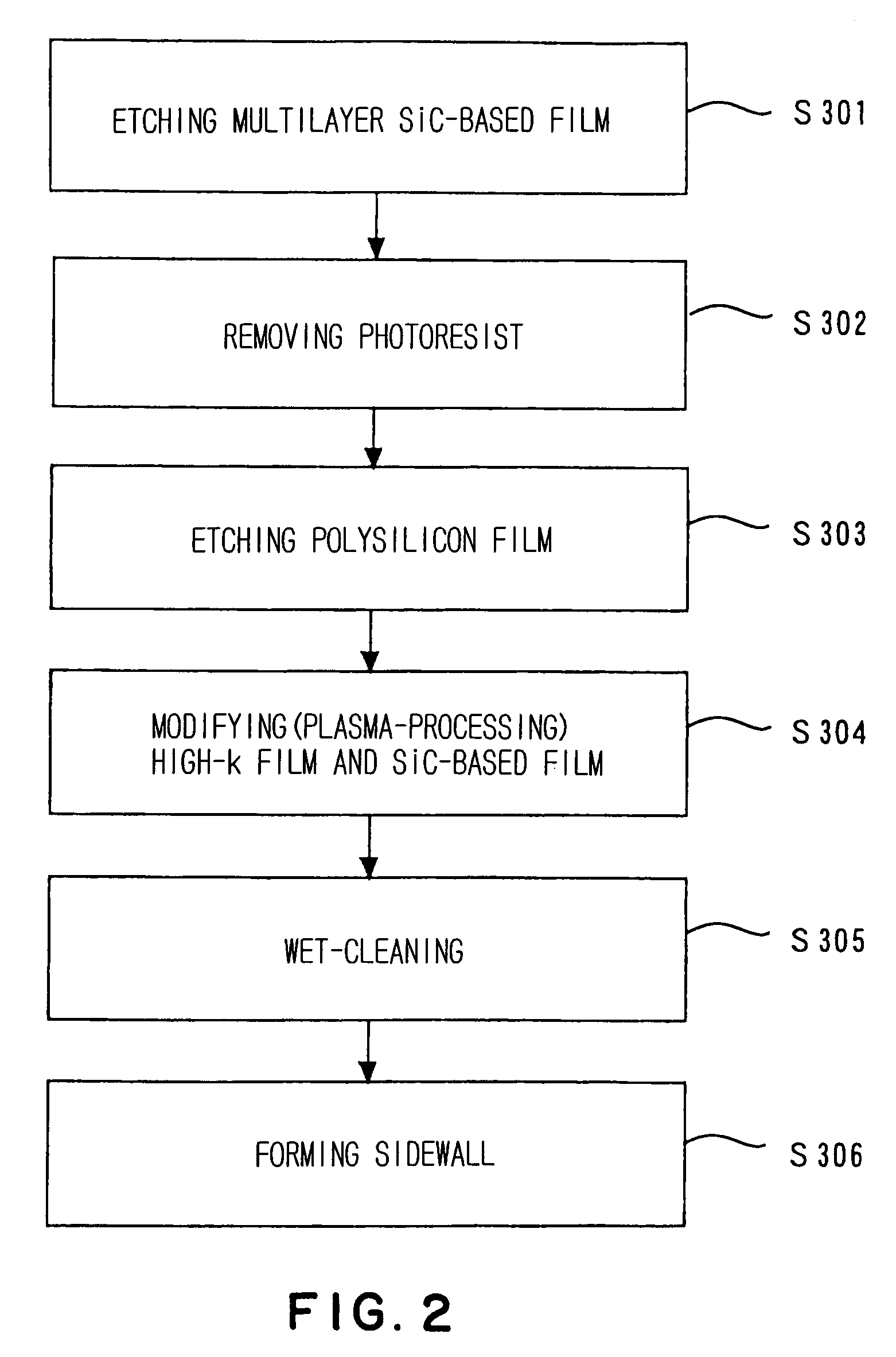
[0035]FIGS. 1A to 1G are schematic views of cross-sections of a wafer in the order of a gate electrode forming process of a MOS transistor in one embodiment of the present invention. FIG. 2 is a flowchart showing major steps in the gate electrode forming process shown in FIGS. 1A to 1G.

[0036]FIG. 1A shows a layered body structure of a gate forming part before it is etched. On a silicon substrate 101 forming a semiconductor wafer W, there is formed as a gate insulation film a High-k film 102 made of, e.g., HfO2 or HfSiOx. The High-k film 102 may be formed by a CVD, for example. On the High-k film 102, there is formed a polysilicon film 103 by a CVD, for example. On the polysilicon film 103, there is formed an SiC-based film 106 made of, e.g., SiCH and SiCOH. Further, on the SiC-based film 106, a patterned photores...


PUM


Abstract

The present invention is a method of manufacturing a semiconductor device from a layered body including: a semiconductor substrate; a high dielectric film formed on the semiconductor substrate; and an SiC-based film formed on a position upper than the high dielectric film, the SiC-based film having an anti-reflective function and a hardmask function. The present invention comprises a plasma-processing step for plasma-processing the SiC-based film and the high dielectric film to modify the SiC-based film and the high dielectric film by an action of a plasma; and a cleaning step for wet-cleaning the SiC-based film and the high dielectric film modified in the plasma-processing step to collectively remove the SiC-based film and the high dielectric film.

Description

FIELD OF THE INVENTION[0001]The present invention relates to a method of manufacturing a semiconductor device.BACKGROUND ART[0002]With the spread of mobile products represented by cell phones, miniaturization of an LSI has been developed in order to further accelerate a processing speed and to further save a power consumption. There is a tendency that the thickness of a gate insulation film of a transistor is further reduced in accordance with the miniaturization of an LSI.[0003]A silicon oxide film (SiO2) has been conventionally used as a gate insulation film of a MOS transistor. However, a silicon oxide film having a thickness of not more than 2 nm has a poor insulation performance, so that a leak current is increased. With increase in the gate leak current, a power consumption is significantly increased. When such a gate insulation film is employed in a mobile product, an available time of a battery in the mobile product is reduced. In addition, because of a thinner gate insulati...

Claims


Application Information

Patent Timeline
Patent Type & Authority Patents(United States)
IPC IPC(8): H01L21/336H01L21/8234H01L21/4763H01L21/3205H01L21/76
CPCH01L21/28123H01L21/31111H01L21/31144H01L21/32139Y10S438/931H01L21/306
Inventor GALE, GLENNHIROTA, YOSHIHIROMURAKI, YUSUKENAKAMURA, GENJIKUSHIBIKI, MASATOSHINDO, NAOKISHIMIZU, AKITAKAASHIGAKI, SHIGEOKATO, YOSHIHIRO
Owner TOKYO ELECTRON LTD
Why Eureka
Try Eureka