Inductance-tuned circuit board via crosstalk structures
- Summary
- Abstract
- Description
- Claims
- Application Information
AI Technical Summary
Problems solved by technology
Method used
Image

Examples
first embodiment
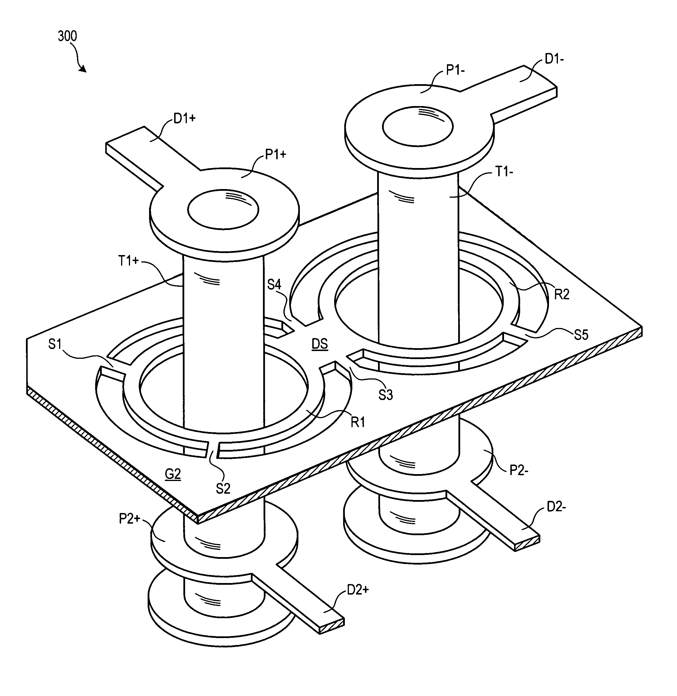
[0025]FIG. 3 illustrates, in perspective view, a partial circuit board assembly 300 according to a Partial circuit board assembly 300 includes a first differential pair, D1+, D1−, connected respectively to a second differential pair, D2+, D2−, through a path comprising a first pair of pads P1+, P1−, a pair of PTHs T1+, T1−, and a second pair of pads P2+, P2−. PTHs T1+, T1− pass through a ground plane G2 that lies intermediate the signal layers containing the two sets of differential pairs and pads.
[0026]A collar / spoke arrangement provides the ground plane coupling from PTHs T1+, T1− to the adjacent portions of ground plane G2. The collar / spoke arrangement comprises a conductive ring R1 around T1+, separated by a clearance, a conductive ring R2 around T1−, separated by a clearance, a thick differential spoke DS in the region between the two PTHs, and six smaller spokes (S1, S2, S3, S4, S5, and a sixth spoke from R2 to G2, the sixth spoke occluded in FIG. 3 by T1−). Spoke DS connects...
second embodiment
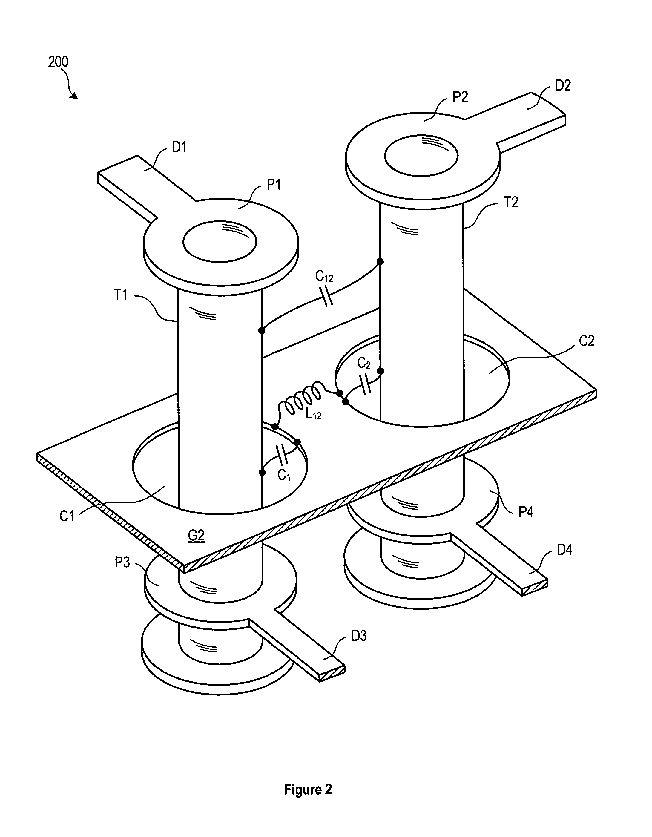
[0027]FIG. 4 illustrates, in perspective view, a partial circuit board assembly 400 according to a Partial circuit board assembly 400 includes an aggressor signal path from a stripline conductor A1 on one signal layer to another stripline conductor A2 on another signal layer, and a victim signal path from a stripline conductor V1 on one signal layer to another stripline conductor V2 on another signal layer (the signal layers used for both signal paths are shown the same, but this is not necessary to the embodiment). The aggressor signal path comprises stripline conductor A1 connected to a pad P1, connected in turn to a PTH T1, connected in turn to a pad P3, and connected in turn to a stripline conductor A2. The victim signal path comprises stripline conductor V1 connected to a pad P2, connected in turn to a PTH T2, connected in turn to a pad P4, and connected in turn to a stripline conductor V2. Signals on the aggressor signal path can couple as noise to the victim signal path due ...
embodiment 1300
[0043]FIG. 13 shows in perspective view an exemplary application of the collar / spoke arrangement of FIG. 11D in a multi-ground plane embodiment 1300. A PTH T1 passes through four ground planes G1, G2, G3, and G4. The FIG. 11D directional spoke arrangement and its mirror image are applied alternately between successive ground planes. In the alternative, the directional spoke arrangement can be the same orientation in each ground plane, e.g., to support transmission of signals in one direction and oppose noise transmission in the opposite direction.
[0044]Another alternate feature, the use of nonfunctional pads, is depicted in FIG. 13. On ground planes G1 and G4, PTH T1 passes through a nonfunctional pad centered in the clearance. The nonfunctional pads add capacitance to the coupling between the PTH and the collar on the ground planes on which they are deployed, providing another way to customize the PTH impedance.
[0045]FIG. 14 shows in perspective view an exemplary application of the...
PUM
 Abstract
Description
Claims
Application Information
 - R&D
- Intellectual Property
- Life Sciences
- Materials
- Tech Scout
- Unparalleled Data Quality
- Higher Quality Content
- 60% Fewer Hallucinations
Browse by: Latest US Patents, China's latest patents, Technical Efficacy Thesaurus, Application Domain, Technology Topic, Popular Technical Reports.
© 2025 PatSnap. All rights reserved.Legal|Privacy policy|Modern Slavery Act Transparency Statement|Sitemap|About US| Contact US: help@patsnap.com