Substrate for semiconductor device and manufacturing method thereof

a technology of semiconductor devices and substrates, which is applied in the direction of semiconductor devices, semiconductor/solid-state device details, electrical apparatus, etc., can solve the problems of difficult general substrate implementation of recent trends, deterioration of electrical efficiency of semiconductor devices using electrically conductive patterns, and thickening of semiconductor devices using substrates. , to achieve the effect of improving electrical efficiency, thin thickness and shortening of electrically conductive patterns

Active Publication Date: 2011-03-08
AMKOR TECH SINGAPORE HLDG PTE LTD
View PDF469 Cites 188 Cited by
  • Summary
  • Abstract
  • Description
  • Claims
  • Application Information

AI Technical Summary

Benefits of technology

[0008]A substrate for a semiconductor device and a manufacturing thereof, and a semiconductor device using the same and a manufacturing method thereof are disclosed. For example, in the substrate according to the present invention, a core is eliminated, so that the substrate has a very thin thickness, as well, the length of electrically conductive patterns becomes shorter, whereby the electrical efficiency thereof is improved. Moreover, since a carrier having a stiffness of a predetermined strength is bonded on the substrate, it can prevent a warpage phenomenon during the manufacturing process of the semiconductor device. Furthermore, the carrier is removed from the substrate, whereby a solder ball fusing process or an electrical connecting process of the semiconductor die can be easily performed.

Problems solved by technology

However, since such substrate is comparatively thicker, there is a defect in that the thickness of the semiconductor device using the substrate becomes thicker.
Also, because each electrically conductive pattern of the substrate is comparatively longer, there is a defect in that the electrical efficiency of the semiconductor device using the electrically conductive patterns is deteriorated.
However, it is difficult for the general substrate to implement recent trends thereof.
However, where the core layer is eliminated from the substrate, since the warpage phenomenon is very higher during the manufacturing process of the semiconductor, it is difficult to manufacturer the semiconductor device.
Also, it is difficult to manufacture and handle the substrate owing to the low stiffness thereof.

Method used


Image

  • Substrate for semiconductor device and manufacturing method thereof
  • Substrate for semiconductor device and manufacturing method thereof
  • Substrate for semiconductor device and manufacturing method thereof

Examples


Embodiment Construction

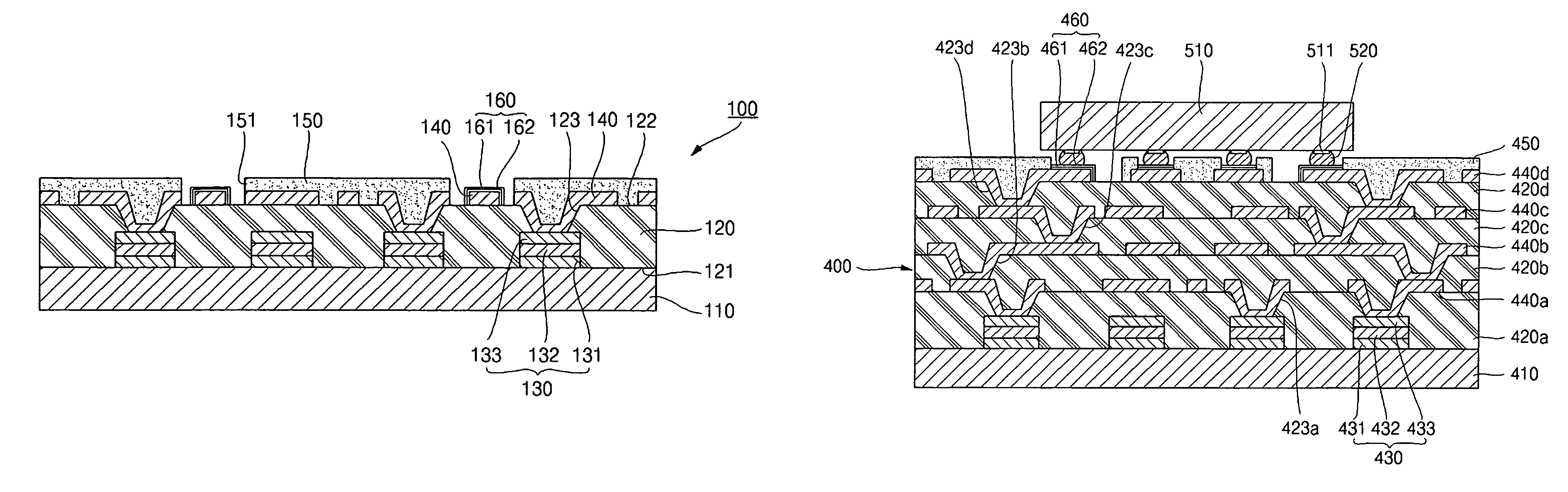
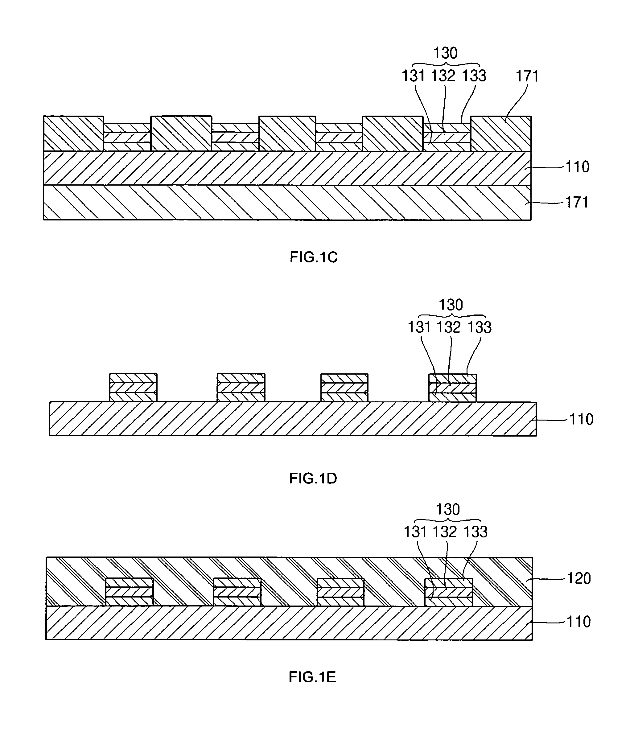
[0070]Referring to FIG. 1, a sectional view of a substrate 100 for a semiconductor device according to one embodiment of the present invention is illustrated.

[0071]As shown in FIG. 1, the substrate 100 for a semiconductor device includes a carrier 110 having a predetermined stiffness, a dielectric layer 120 formed on the carrier 110, a plurality of conductive lands 130 electrically connected to the carrier 110 at the inside of the dielectric layer 120, a plurality of electrically conductive patterns 140 electrically connected to the conductive lands 130 at the surface of the dielectric layer 120, and a solder mask 150 for covering the dielectric layer 120 and the electrically conductive patterns 140, a predetermined area of each conductive pattern 140 being exposed to outside.

[0072]The carrier 110 is in the form of an approximately planar plate. The material of the carrier 110 may be a metal, a film or its equivalent, in order that a warpage is not generated during the manufacturing...


PUM


Abstract

A substrate for a semiconductor device and a manufacturing thereof, and a semiconductor device using the same and a manufacturing method thereof are disclosed. For example, in the substrate according to the present invention, a core is eliminated, so that the substrate has a very thin thickness, as well, the length of electrically conductive patterns becomes shorter, whereby the electrical efficiency thereof is improved. Moreover, since a carrier having a stiffness of a predetermined strength is bonded on the substrate, it can prevent a warpage phenomenon during the manufacturing process of the semiconductor device. Furthermore, the carrier is removed from the substrate, whereby a solder ball fusing process or an electrical connecting process of the semiconductor die can be easily performed.

Description

BACKGROUND OF THE INVENTION[0001]1. Field of the Invention[0002]The present invention relates to substrate for semiconductor device and manufacturing method thereof, and semiconductor device using the same and manufacturing method thereof.[0003]2. Description of the Related Art[0004]Generally, a semiconductor device includes a substrate having a plurality of electrically conductive patterns thereon, a semiconductor die located on the substrate, a plurality of conductive connecting means for electrically connecting the substrate to the semiconductor die, and an encapsulant for encapsulating the semiconductor die and the conductive connecting means. Here, a plurality of solder balls can be further fused to the substrate so as to electrically connect the semiconductor device to an external device.[0005]Meanwhile, a relatively thick core layer is formed at the substrate of the semiconductor device, in order that a warpage is not generated during the manufacturing process of the semicond...

Claims


Application Information

Patent Timeline
Patent Type & Authority Patents(United States)
IPC IPC(8): H01L23/04
CPCH01L21/4857H01L21/563H01L21/6835H01L23/3128H01L23/498H01L23/49822H01L23/49894H01L24/16H01L24/32H01L24/81H01L23/49816H01L24/48H01L2221/68345H01L2224/0401H01L2224/05568H01L2224/13099H01L2224/16225H01L2224/16237H01L2224/32057H01L2224/32225H01L2224/48091H01L2224/48227H01L2224/48228H01L2224/73203H01L2224/73204H01L2224/73265H01L2224/81001H01L2224/81801H01L2224/83385H01L2224/92247H01L2924/01013H01L2924/01029H01L2924/01078H01L2924/01079H01L2924/09701H01L2924/15311H01L2924/30105H01L2924/01033H01L2924/014H01L2224/45124H01L2224/45144H01L2224/48599H01L2224/48699H01L2924/0002H01L2924/00014H01L2924/00012H01L2924/00H01L2224/05552H01L24/45H01L24/73H01L2924/181
Inventor LEE, KYU WONPARK, DOO HYUNKANG, DONG HEE
Owner AMKOR TECH SINGAPORE HLDG PTE LTD
Why Eureka
Try Eureka