Clock gating system and method

a clock gating and clock technology, applied in the field of clock gating, can solve the problems of reducing the user's experience, consuming a large portion of clock gating power, and reducing so as to reduce the power consumption reduce the footprint of clock gating circuits

Active Publication Date: 2011-03-08
QUALCOMM INC
View PDF25 Cites 44 Cited by
  • Summary
  • Abstract
  • Description
  • Claims
  • Application Information

AI Technical Summary

Benefits of technology

[0005]In a particular embodiment, a clock gating system incorporates circuitry that functions as a set-reset latch instead of a traditional pass-gate latch to hold an enable signal on clock gating circuitry. The set-reset latch includes a pair of cross-coupled NOT-AND (NAND) gates. One of the NAND gates is merged with the NAND gate blocking the clock. The clock gating system can reduce the number of transistors and have a smaller area compared to a cell using pass-gate latch. The clock gating system can also reduce the number of transistors that always toggle when the clock signal toggles, reducing the dynamic power consumption as compared to a conventional clock gating cell.
[0010]One particular advantage provided by at least one of the disclosed embodiments is reduced power consumption of clock gating circuits. Another particular advantage provided by at least one of the disclosed embodiments is a reduced footprint of clock gating circuits. Another particular advantage provided by at least one of the disclosed embodiments is that fewer transistors switch with each clock cycle.

Problems solved by technology

However, power consumption of such portable devices can quickly deplete a battery and diminish a user's experience.
The clock tree often consumes a significant portion of the power consumed by a semiconductor device, and unnecessary power consumption can occur in a branch of a clock tree when the output of the branch is not needed.
However, clock gating cells that are used to perform clock gating also consume power.

Method used


Image

  • Clock gating system and method
  • Clock gating system and method
  • Clock gating system and method

Examples


Embodiment Construction

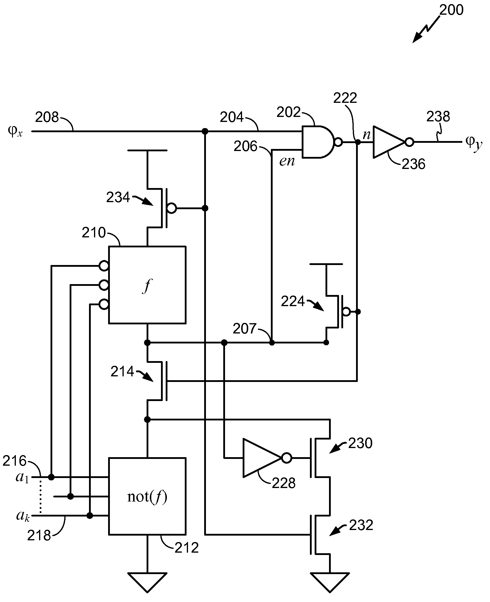
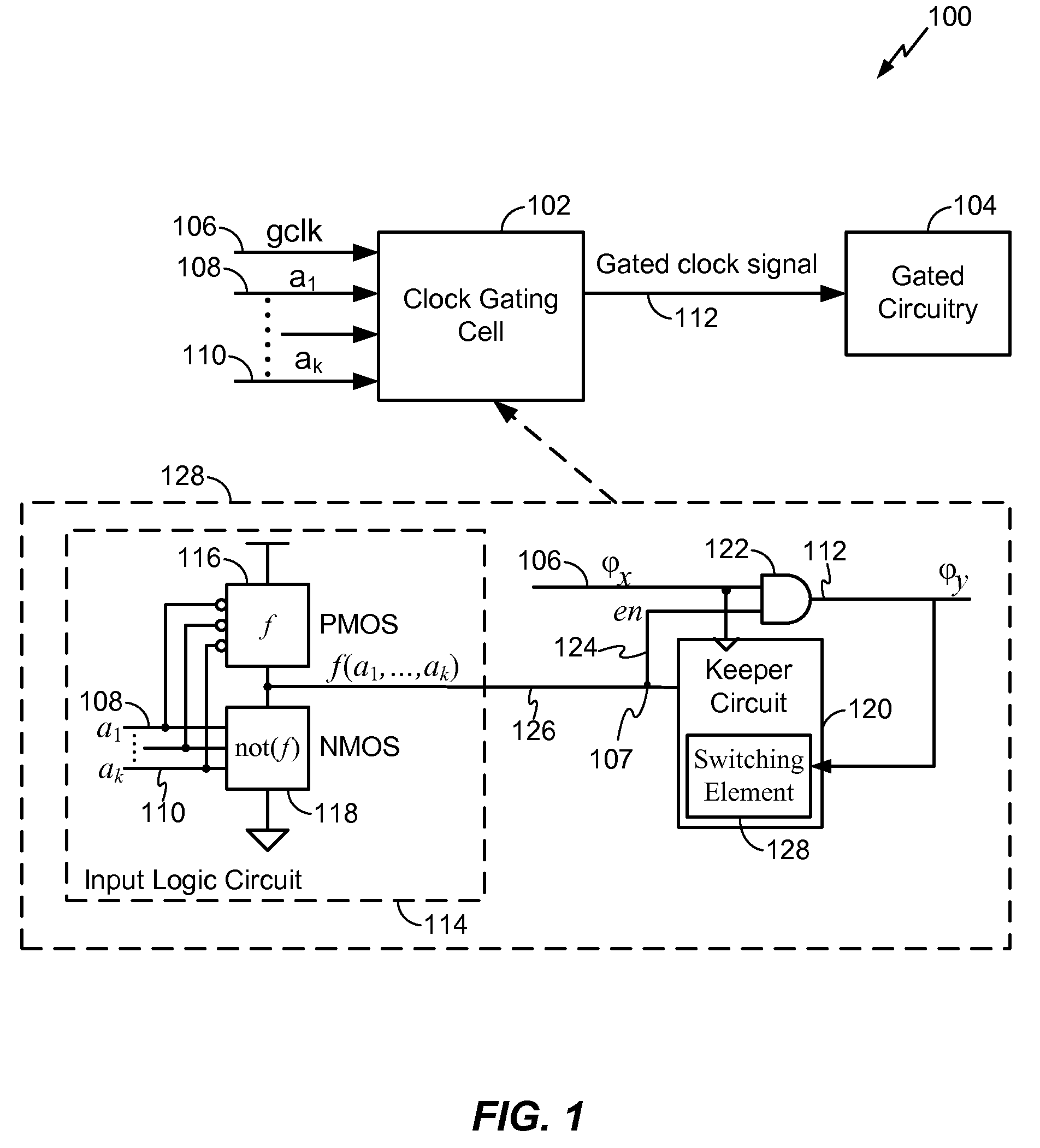
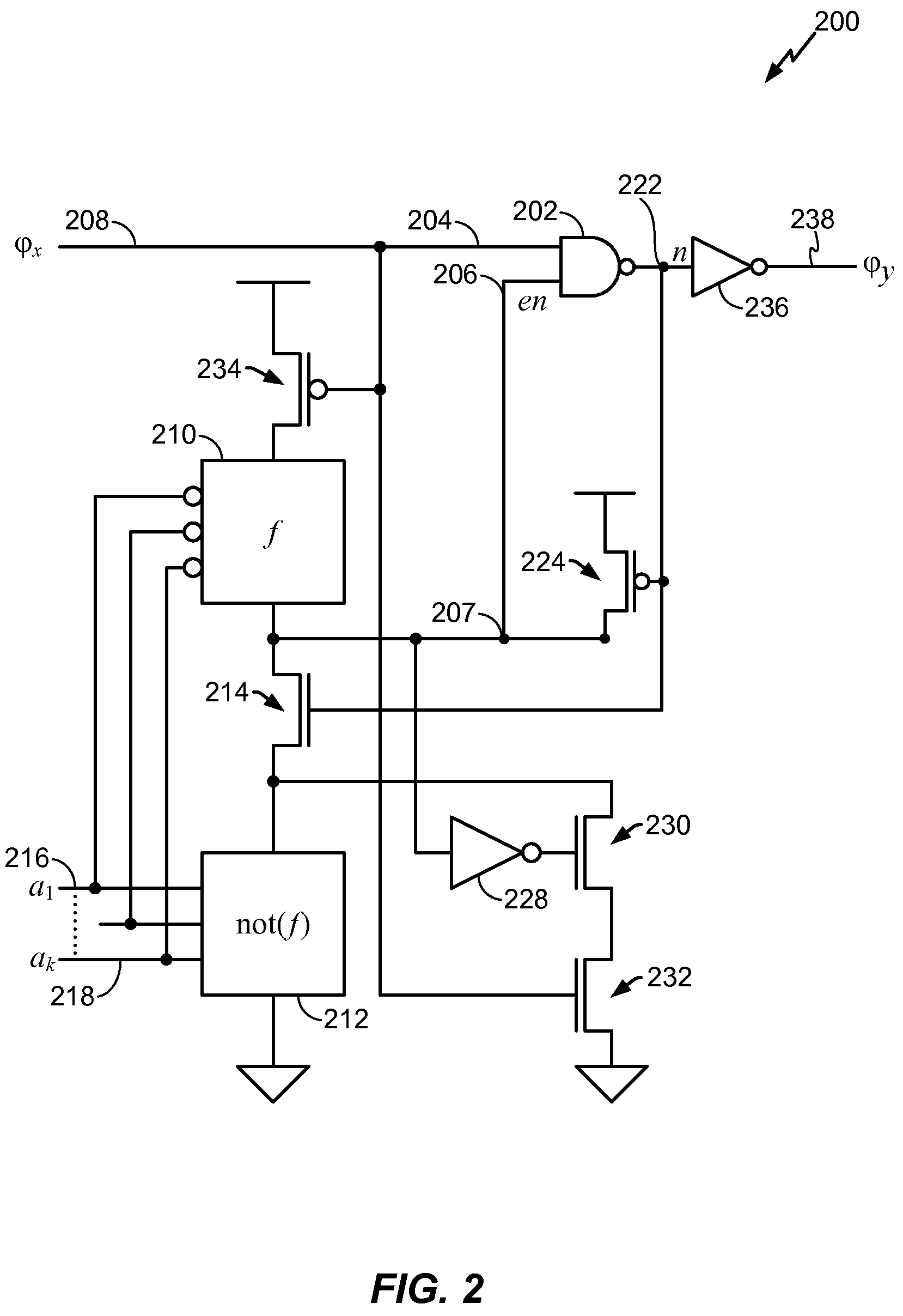
[0018]Referring to FIG. 1, an illustrative embodiment of a system to generate a gated clock signal is depicted and generally designated 100. The system 100 includes a clock gating cell 102 coupled to gated circuitry 104. The clock gating cell 102 receives a clock input 106 and a first input 108. The clock gating cell 102 may also receive one or more additional inputs, such as a second input 110. The clock gating cell 102 provides a gated clock signal 112 to the gated circuitry 104. The clock gating cell 102 contains a clock gating circuit 128.

[0019]The clock gating circuit 128 contains an input logic circuit 114 coupled to an internal enable node 107. A keeper circuit 120 and a gating element 122 are also coupled to the internal enable node 107. The keeper circuit 120 includes at least one switching element 128 that is responsive to the gated clock signal 112. Because the switching element 128 is responsive to the gated clock signal 112 instead of a input clock signal received at th...


PUM


Abstract

A clock gating system and method is disclosed. In a particular embodiment, the system includes an input logic circuit having at least one input to receive at least one input signal and having an output at an internal enable node. A keeper circuit includes at least one switching element that is responsive to a gated clock signal and is coupled to the internal enable node to selectively hold a logical voltage level at the internal enable node. The system further includes a gating element responsive to an input clock signal and to the logical voltage level at the internal enable node to generate the gated clock signal.

Description

I. CROSS-REFERENCE TO RELATED APPLICATION(S)[0001]The present disclosure claims the benefit of U.S. Provisional Application No. 61 / 048,661, filed Apr. 29, 2008, which is incorporated by reference herein in its entirety and to which priority is claimed.II. FIELD[0002]The present disclosure is generally related to clock gating.III. DESCRIPTION OF RELATED ART[0003]Advances in technology have resulted in smaller and more powerful personal computing devices. For example, there currently exist a variety of portable personal computing devices, including wireless computing devices, such as portable wireless telephones, personal digital assistants (PDAs), and paging devices that are small, lightweight, and easily carried by users. More specifically, portable wireless telephones, such as cellular telephones and Internet Protocol (IP) telephones, can communicate voice and data packets over wireless networks. Further, many such wireless telephones include other types of devices that are incorpo...

Claims


Application Information

Patent Timeline
Patent Type & Authority Patents(United States)
IPC IPC(8): H03K19/096
CPCH03K19/0016G06F1/04
Inventor SAINT-LAURENT, MARTINMOHD, BASSAM JAMILBASSETT, PAUL
Owner QUALCOMM INC
Why Eureka
Try Eureka